In clear sight: How a UK-Israel programme lifted my research
An Israeli researcher describes her experience at the University of Oxford, after being awarded a Science and Innovation Researcher Mobility fellowship.
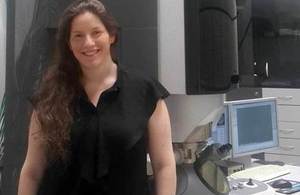
Hadas Sternlicht, PhD student at the Department of Materials Science and Engineering at the Technion, Israel Institute of Technology.
Collaborations are a powerful and essential tool in scientific research. They offer new insights into already existing results, and allow one to quickly learn important aspects on a topic of interest.
About two years ago, when Prof. Angus Kirkland from the University of Oxford gave a talk at the Technion– Israel Institute of Technology, where I work on my PhD, an opportunity for such a collaboration was arising. A few months later, I received an email from my advisor, Prof. Wayne D. Kaplan, informing me about funding opportunities offered by the UK’s Science and Innovation Network in Israel.
I chose the Researcher Mobility Fellowship Scheme. This program is designed to enable early career researchers in Israel or the UK who work in one of the British Embassy’s scientific priority areas: nanotechnology, neuroscience, water and agriscience and regenerative medicine, to conduct a research visit to Israel or the UK of up to six months to focus on developing research links and scientific collaborations.
When I first visited the UK, as a 12 years old girl, I visited the Toy Museum in London. Now, I had a chance to return to the UK as an adult, as part of my PhD studies, to “play” with a new kind of toys: electron microscopes. I thought this could be a great opportunity for me to work on one of the challenges associated with my research, which focuses on the mechanism of grain boundary motion.
Most engineering materials are polycrystalline, where the crystals they are made of are often called “grains”, and the plane of contact between crystals is called a grain boundary. While control of the grain size is required to control many of the engineering properties of polycrystalline materials, the atomistic mechanism by which grain boundaries move is not known. As such, in my research general grain boundaries were characterized using transmission electron microscopy (TEM), which enables atomic resolution.
So during the summer of 2015, I spent a month at the University of Oxford working with Prof. Angus Kirkland and his group. During this visit, I studied software that was written by Prof. Kirkland and his group, which enables us to gain more information from the microscope, using sets of images where each image is recorded at different value of focus or orientation of the electron beam.
Analysis of such sets of images provides more information than single images regarding the local position of atoms in a sample, and eliminate (to some extent) distortions, which are inherent in the imaging system of electron microscopes. Such analysis enabled me to better understand the structure of steps at the grain boundaries.
During this visit, I had the opportunity to interact with experts in the field of microscopy. We had fruitful discussions about my research in general, and discussed the structure of grain boundaries in light of the resulting information arising from the analysis done using the software. It was pleasant to conduct open discussions with them, and freely ask questions. I was allowed to join their group meeting which took place during my visit, and had the opportunity to look at some of my samples using their microscope. Overall, it was a very useful and enjoyable month, which was possible due to the excellent programmes of the Science and Innovation Network.
Further information
Ms. Sternlicht is a PhD student at the Department of Materials Science and Engineering at the Technion – Israel Institute of Technology.