Semiconductor sector study 2026
Updated 2 September 2026

© Crown copyright 2026
This publication is licensed under the terms of the Open Government Licence v3.0 except where otherwise stated. To view this licence, visit nationalarchives.gov.uk/doc/open-government-licence/version/3 or write to the Information Policy Team, The National Archives, Kew, London TW9 4DU, or email: psi@nationalarchives.gov.uk.
Where we have identified any third party copyright information you will need to obtain permission from the copyright holders concerned.
This publication is available at https://www.gov.uk/government/publications/semiconductor-sector-study-2026/semiconductor-sector-study-2026
Executive summary
This report presents findings from research undertaken to produce an updated analysis of semiconductor-related economic activity in the UK. Commissioned by the Department for Science, Innovation and Technology (DSIT) in 2026, the study is intended to enable a better understanding of the composition, scale, opportunities and challenges affecting semiconductor-related activity in the UK.
-
Semiconductors are foundational infrastructure for the 21st century economy, enabling markets worth over $10 trillion globally and underpinning every UK priority growth sector identified in the UK’s Modern Industrial Strategy, particularly advanced manufacturing, digital and technologies, clean energy and defence. Global semiconductor sales have grown by 39% since 2022 to $796bn in 2025, driven primarily by AI compute[footnote 1].
-
The study identifies 703 UK semiconductor companies (295 dedicated, 408 diversified), up from 623 at baseline[footnote 2]. 70% of dedicated companies are UK-headquartered and 92% are SMEs; activity remains concentrated in twelve recognised regional clusters spanning design strength (Cambridge, London, Bristol, Southampton) and manufacturing or materials depth (South Wales, Scotland, North East).
-
Dedicated companies generated an estimated £10.6bn in revenue, £7.5bn in GVA and directly employed approximately 16,350 people in 2025 - up 7%, 9% and 9% respectively since the baseline study. The sector is estimated to support up to 32,550 jobs across the economy.
-
Economic activity is concentrated within a small number of large companies, which are estimated to account for 75% of revenue and 61% of employment (up from approx. 66% and 53%).
-
There is evidence of greater government support for the sector since the publication of the National Semiconductor Strategy, at both national and regional levels, spanning R&D, skills and use of public finance institutions.
-
Investment activity has been strong since the 2024 study. Grants and fundraising across the baseline cohort increased by 16% to £1.73bn, with newly identified dedicated companies securing a further £400m - heavily weighted to design-led, seed or venture-stage firms in the East of England, London and the South East.
-
Industry sentiment remains overwhelmingly positive - 83% of surveyed firms expect growth over the next three years and 47% expect rapid growth of 20% p.a. (up from 38% in 2024) - but persistent barriers risk constraining delivery, including the availability of talent, access to scale-up capital, and UK operating costs, particularly energy.
1. Introduction and background
DSIT commissioned Perspective Economics (PE) and a consortium of advisors including TechWorks (TW), IfM Engage (IfM), the UK Electronic Skills Foundation (UKESF) and independent technologists to conduct a follow-up study into the UK semiconductor sector published in 2024. The research presented in this report seeks to provide further detail regarding semiconductor sectoral activity in the UK.
1.1 Study objectives
This second iteration of the semiconductor sector study seeks to build on the baseline sector study to further DSIT’s understanding of the UK semiconductor sector, including:
-
How much the UK’s semiconductor sector contributes to the UK economy?
-
What the UK’s position is within international semiconductor trade?
-
How mature or dynamic the UK semiconductor sector is?
-
What the implications of UK semiconductor activity are on other UK policy areas?
-
What the future trends, risks and opportunities may be for the UK semiconductor sector?
1.2 Methodology and approach
The study follows an approach that is consistent with, and builds upon, that used to produce the baseline semiconductor sector study, and similar evidence regarding the UK’s cyber security and artificial intelligence (AI) sectors. The approach is summarised in Figure 1.1 below and described in detail in the report appendices.
Figure 1.1 – Overview of method
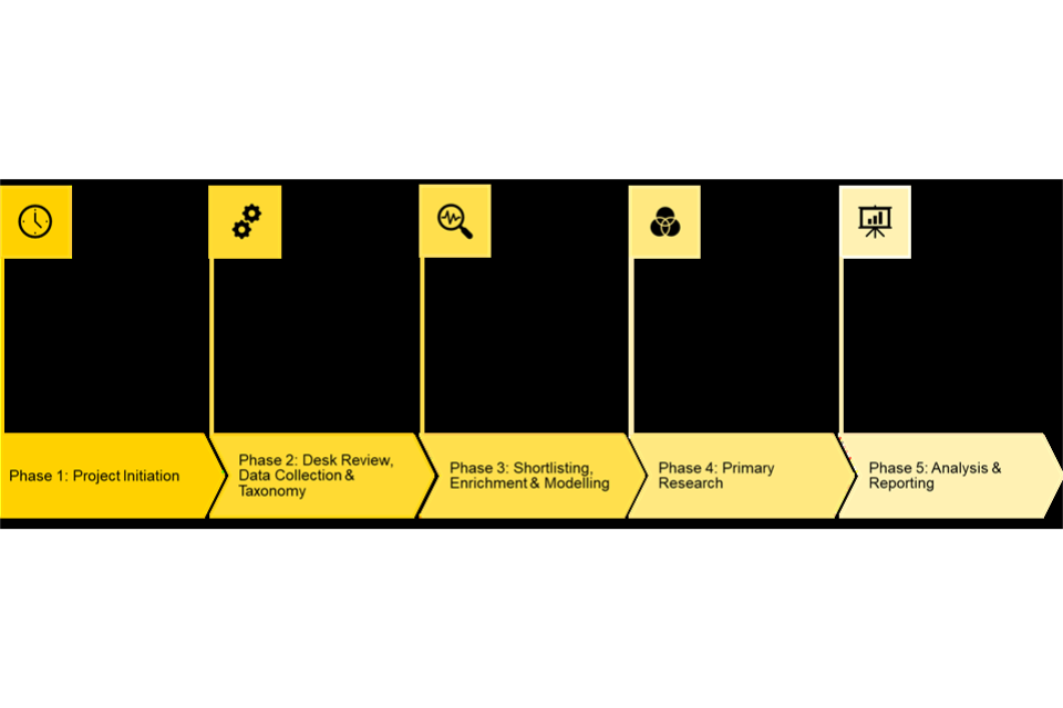
The overall approach and methodology used to produce this iteration of the study is consistent with the 2024 version but the analytical tools and techniques available to gather and analyse sectoral evidence have continued to evolve.
1.3 Acknowledgements
The study team would like to extend its sincere thanks to its panel of expert advisors, and to all who gave their time to contribute to the research by completing the survey, or taking part in consultations and / or workshops.
2. Semiconductor-enabled industries
Semiconductors are highly specialized components that provide the essential functionality for electronic devices to process, store and transmit data[footnote 3]. Most of today’s semiconductors are integrated circuits, also referred to as “chips” composed of active discrete devices, passive devices and the interconnections between them, layered on a thin wafer of semiconductor material.
Semiconductors are a marvel of modern technology and the foundation of our digital world.
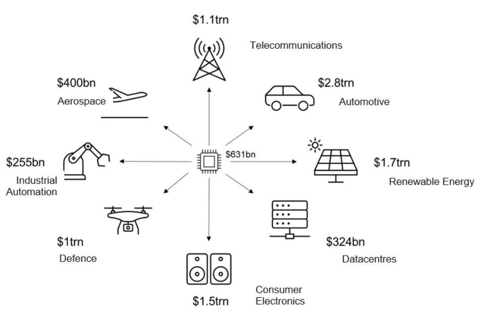
Semiconductor technology underpins virtually every modern industry, acting as a foundational, enabling capability which drives economic growth, productivity and innovation in that industry. From computing infrastructure and telecommunications to automotive, healthcare, defence and energy systems; semiconductors provide the processing, sensing, power management and connectivity functions that define how products and services operate. As digitalisation, automation and ubiquitous connectivity accelerate, the demand for semiconductor technologies is increasing rapidly, reflecting their central role in enabling real-world systems. Recently published global estimates for markets to which semiconductors are integral total more than $10trn (Figure 2.1), including aerospace, industrial automation, defence, consumer electronics, compute, renewable energy, automotive and telecommunications[footnote 4].
Figure 2.1 – Semiconductor enabled global markets
Source: Perspective Economics, Various (*SIA 2025 State of Semiconductor Industry)
Innovations in semiconductor technology and devices are the fuel powering major emerging transformational technologies, including AI, automation, robotics, future communications, med-tech and clean energy. None of these sectors can exist without advances in semiconductor performance, efficiency and integration.
In the age of AI, it’s often said that data is the new oil. Yet the real limitation we face isn’t the availability of data, it’s processing power.
Semiconductors are the backbone of AI systems, driving their computational power and efficiency. The immense computational demands of AI tasks, like training complex machine learning models or processing real-time data, far exceed the capabilities of traditional computer processors. This has led to the development of specialised processors and custom AI accelerators specifically designed to handle AI workloads. These AI-focussed processors rely on cutting-edge semiconductor technology[footnote 5]. In the automotive sector, semiconductors are central to the transition toward electrification and autonomous driving, enabling power management, battery control, advanced driver assistance systems, and in-vehicle connectivity. Telecommunications infrastructure, including 5G and emerging 6G networks, depends on advanced chips to deliver high-speed, low-latency connectivity that underpins digital economies. Similarly, in energy systems, semiconductors are critical for efficient power conversion, grid sensing and management, and the integration of renewable energy sources.
For the UK, this makes semiconductor capability a matter of strategic economic importance. As well as being a significant source of economic value in their own right, generating high-value jobs, strong productivity gains and widespread spillover benefits across the wider economy, semiconductors are critical to the UK’s priority growth sectors. Advanced manufacturing, digital technologies, clean energy and defence are all either directly driven by, or critically dependent on, semiconductor technology.
Without a strong domestic ecosystem spanning design, materials, equipment and specialised manufacturing, the UK risks constraining its ambitions in these sectors and increasing reliance on external supply chains in a geopolitically uncertain environment.
Industry Stakeholder
3. Sector profile
Since the previous sector study was published in 2024, semiconductors have been identified as one of the five critical technologies identified within DSIT’s science and technology framework[footnote 6], and as one of six ‘frontier technologies’ within the UK Industrial Strategy[footnote 7].
Semiconductors underpin all of the other five strategically significant technologies, including artificial intelligence and quantum technologies. This recognition provides a foundation from which the UK semiconductor sector can further build. Since the publication of the National Semiconductor Strategy in 2023, greater government support for the sector has been evident at both national and regional levels, spanning R&D, skills and use of public finance institutions. Table 3.1 below explains how semiconductor companies are defined for the purposes of the study, including with respect to the primary focus of company activity, the geographic footprint of in-scope companies and the size of in-scope companies.
Table 3.1 – Semiconductor company definitions
| Parameter | Type | Definition |
|---|---|---|
| Company activity | Dedicated | Companies that specialize in the design, development, and manufacture of semiconductors, or in the provision of materials exclusively to the semiconductor sector. Including companies across the semiconductor supply chain spanning design, materials and manufacturing that have at least one technical employee in the UK. To avoid inflating estimates of productive UK activity the definition of ‘dedicated’ semiconductor companies excludes large companies that do not undertake any design or manufacturing activity in the UK. |
| Company activity | Diversified | Companies operating across a wide range of industries and sectors, of which the semiconductor industry is one. In-scope companies must have descriptive evidence of active engagement in semiconductor-related activity e.g., supply of products or services to the semiconductor industry, ongoing semiconductor related research or development / integration of chips as part of a broader product or service offering. These companies may have technical semiconductor employees but technical employment is not a pre-requisite for inclusion. |
| Geographic footprint | UK headquartered | Companies with registered headquarters in the UK and may also have international operations. |
| Geographic footprint | Foreign headquartered | Companies with registered headquarters outside of the UK but with UK operations. |
| Size | SME | Consistent with the Companies Act 2006, the term SME is defined based on UK headcount: Micro companies (1 – 9 employees), Small companies (10 – 49 employees), Medium sized companies (50 – 249 employees). |
| Size | Large | Consistent with the Companies Act 2006 large companies are defined as having staff headcount of more than 250 employees. |
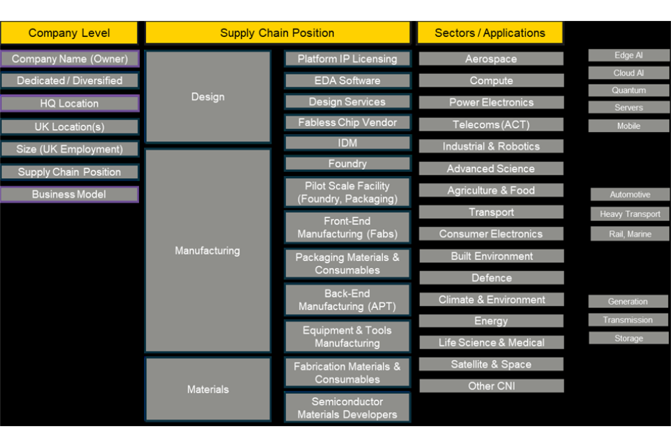
Figure 3.1 overleaf illustrates the taxonomy used to categorise the sector for this year’s study. It builds on the baseline categorisation, seeking to add additional detail regarding supply chain positions, manufacturing capability, materials information, product types and application areas.
Figure 3.1 – High-level semiconductor segmentation (2026)
Source: Perspective Economics, DSIT, Advisory Panel
3.1 Sectoral changes 2022/23 – 2024/25
A review of more than 30 strategic reports filed at Companies House by the UK’s largest dedicated semiconductor companies in late 2024 and early 2025 returned the following observations:
-
Growth driven by AI compute, memory and licensing: Companies involved in AI compute supply chains, memory and licensing performed strongly. Some of the UK’s foremost semiconductor companies grew global revenues substantively due to increased demand for AI-driven design and licensing, hyperscaler demand for GPUs and memory, and increased demand for semiconductor equipment
-
Inventory corrections: Conversely, companies exposed to broad analogue, mixed-signal and consumer end-markets saw reductions in turnover (despite continued underlying demand) as customers continued to work through existing stock
-
Government intervention: Strategic reports provide evidence of UK government support for the sector, at both national and regional levels, spanning R&D, skills, public procurement, and use of public finance institutions
-
Geopolitical risks: Every strategic report flagged geopolitical risk, including trade uncertainties due to the impact of tariffs, US export controls on advanced compute hardware, and international conflicts
-
UK fab and compound-semi capacity investment: Nexperia increased its Manchester 200mm (8-inch) silicon wafer production line by 7% by the end of 2025; Pragmatic Semiconductor opened FlexLogic-003 cleanroom at Durham which is expected to create 500 additional highly skilled jobs by 2030[footnote 8]; Plessey upgraded its 200mm (8-inch) line in Plymouth; and Octric is rebuilding GaN capability with some public finance contributions
-
Talent retention and skills competition: Across all of the strategic reports reviewed, engineering-talent retention and competition for AI-skills were the most-cited human resource risks
Overall, review of annual reports suggests that the semiconductor sector was leaner in FY2025, with a clearer split between companies involved in AI compute and licensing, and those supplying higher-volume markets such as automotive. Since the 2024 study there is evidence of substantive government involvement and increased emphasis among semiconductor companies on geopolitical risks. Sovereign-capability drivers, compound-semiconductor capacity expansion, and AI-related strategic transactions are structural shifts that may prevail across 2025 and 2026.
3.2 Number of semiconductor companies
This second iteration of the study has identified a total of 703 companies involved in the UK semiconductor sector. This includes 295 dedicated semiconductor companies and 408 diversified companies[footnote 9].
Table 3.2 – Dedicated and diversified semiconductor companies
| Dedicated or diversified | 2024 (n, %) | 2026 (n, %) |
|---|---|---|
| Dedicated | 210 (34) | 295 (42) |
| Diversified | 413 (66) | 408 (58) |
| Total | 623 (100) | 703 (100) |
Source: Perspective Economics
Within the dedicated cohort of companies 70% are headquartered in the UK and 30% are headquartered internationally (n=209, 88, baseline 66% and 34% respectively).
Registered companies by size
The overall size profile of all companies identified (both dedicated and diversified) has not changed substantively since the baseline study. 89% of all companies identified are micro, small or medium sized (SME) (baseline = 92%). As in the 2024 study, dedicated semiconductor companies are smaller than diversified companies on average, with 92% of dedicated companies classified as SMEs (baseline = 95%), compared to 88% of diversified companies (baseline = 91%). The 24 companies classified as large in the dedicated segment (8% of 295) account for 75% of estimated UK revenues and 61% of employment (baseline = 63% and 53% respectively)[footnote 10].
There are more micro and small-sized companies among the dedicated cohort (73% of dedicated companies are micro or small-sized (n=215), compared to 66% of diversified companies, n=267). These micro and small-sized semiconductor companies employ approximately 3,000 people and have 13 employees on average.
Figure 3.2 – UK semiconductor size profile
| Estimated size | Dedicated | Diversified |
|---|---|---|
| Large | 8.1% | 12.5% |
| Medium | 19.0% | 22.1% |
| Small | 33.9% | 30.6% |
| Micro | 39.0% | 34.8% |
Source: Companies House, Perspective Economics
Dedicated, UK headquartered companies are typically smaller than their international counterparts. 81% of UK headquartered companies are either micro or small, compared to 54% of internationally headquartered UK entities (baseline = 79% and 55% respectively).
Semiconductor company registrations
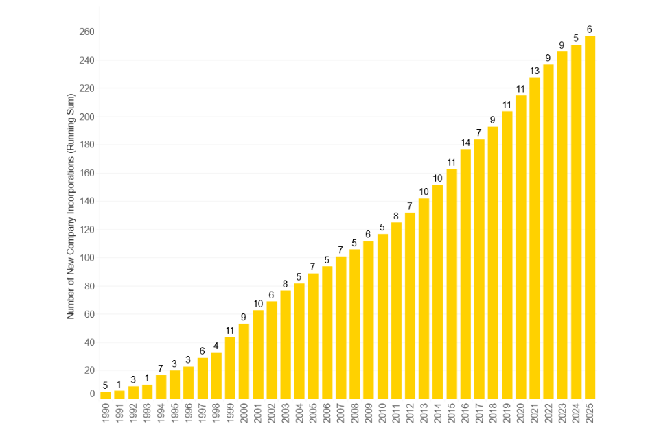
The constant rate of new dedicated company incorporations has continued since the baseline report, with an average of 9 new company incorporations each year since 2016 (baseline average = 8 new incorporations per year). Nine of the 10 new company incorporations in 2024 and 2025 are UK headquartered and are estimated to employ more than 100 people.
Table 3.3 – Example new company incorporations
| Company | Focus |
|---|---|
| Fractile | Fractile is building chips, systems and software to radically improve the speed and cost of running frontier AI inference via a new approach to fusing computation with memory. |
| OLIX Computing | OLIX Computing is developing a new paradigm for AI compute infrastructure through its optical digital processor with a novel memory and interconnect architecture. |
| Novomorphic | Novomorphic designs secure edge AI electronic systems from architecture to silicon where design parameters are constrained by power, thermal limits, RF coexistence, latency or security. |
| Kelvin Quantum | Kelvin Quantum develops semiconductor-based cryogenic-capable electronics (ASICs, integrated circuits, electronic systems) for quantum applications. |
| Chipletti | Chipletti is a fabless semiconductor design company focused on advancing AI inference performance through innovative 3D memory solutions. |
| Convergent Labs | Convergent Labs is building next-generation compound semiconductors for photon-counting imaging applications, including manufacture of CdTe detectors using proprietary crystal growth processes. |
Source: Companies House, Perspective Economics
Figure 3.3 – Semiconductor company incorporations (1990 – 2025)
Source: Companies House, Perspective Economics
3.3 Semiconductor activity by supply chain segment
The study team applied tailored frontier large language model (LLM) scripts to descriptive company information to categorise semiconductor companies according to the supply chain taxonomy set out in Figure 3.1. Categorisations were manually reviewed and updated where relevant based on expert sectoral knowledge. Each dedicated semiconductor company was assigned a ‘best-fit’ supply chain category. While this approach offers a degree of clarity within the analysis, it is recognised that in many cases companies undertake activity across more than one segment of the supply-chain. Table 3.4 provides some illustrations of these overlaps.
Table 3.4 – Design and manufacturing activity overlaps (illustrative)
| Company | Description | Supply chain best fit |
|---|---|---|
| Texas Instruments | Texas Instruments (TI) is a leading global semiconductor company that has been driving progress through innovation for decades. Specializing in the design, manufacture, testing, and sale of analog and embedded processing chips. | Design: Globally Texas Instruments operates across multiple segments of the semiconductor supply chain its UK activity is predominantly R&D related. |
| KLA | KLA (formerly SPTS), is a global leader in designing, manufacturing, selling, and supporting advanced etch, deposition, and thermal processing equipment and technologies for the semiconductor and microdevice industries. | Manufacturing: Globally SPTS is involved in the design and manufacture of semiconductor equipment and tools. The company undertakes both R&D and manufacturing activity in the UK. The company has significant manufacturing activity at its Newport site. |
| Dynex Semiconductor | Dynex Semiconductor Ltd specializes in designing, manufacturing, and supplying high and low power semiconductor devices and modules, including power diodes, thyristors, IGBT modules, and integrated power assemblies. | Manufacturing: Dynex undertakes both R&D and manufacturing activity in the UK. The company has significant manufacturing activity at its Lincoln site. |
| IQE | Specializing in the development, manufacture, and supply of compound semiconductor wafers, IQE leverages advanced epitaxy technology to produce bespoke ‘epi-wafers’ tailored to specific electronic or optical properties required by major chip manufacturers. | Materials: IQE is a leading global supplier of advanced semiconductor materials (wafer products) and services. It also has several manufacturing sites across the UK. |
| STMicroelectronics | STMicroelectronics is a leading global semiconductor company that designs, manufactures, and markets a wide array of microelectronics products, focusing on delivering intelligent and energy-efficient solutions. | Design: STMicroelectronics is a multinational company headquartered in Switzerland. It has manufacturing sites across Europe and Asia and a strong R&D presence in the UK. |
Source: Perspective Economics
Acknowledging the ‘best-fit’ caveat, the supply chain analysis suggests that:
-
60% of dedicated semiconductor companies active in the UK are primarily involved in research and development, design and IP related activities (n=177, baseline 67% n=140)[footnote 11]. Example companies include Arm, Synopsys, Ensilica, Cambridge GaN, XMOS, Novomorphic, Chipletti
-
32% are involved primarily in semiconductor manufacturing activity, including both front and back-end manufacturing and the manufacture of semiconductor equipment and tools. Example companies include KLA, Vishay, Diodes, Seagate, Clas-SIC Wafer Fab, Pragmatic Semiconductor, CIL, Octric, and RAM Innovations (n=94, baseline 28% n=59)
-
8% are primarily involved in the supply of materials to front or back-end manufacturing. Example companies include Shin-Etsu, IQE, Porotech, Photronics, and SmartKem (n=24, baseline 5% n=11)
As in the 2024 study, the supply chain profile of dedicated, UK headquartered companies is not significantly different to these overall proportions. 60% of UK headquartered companies are primarily involved in research, development, design and IP activities, 31% are involved in manufacturing and 9% are involved in the provision or development of semiconductor materials.
The baseline study noted that the UK has a substantive cohort of companies involved in the manufacture of equipment and tools used by the semiconductor sector in the UK, and internationally. Analysis of SME company counts across the updated dataset (including both dedicated and diversified SMEs) reinforces the significance of this segment in the UK. Figure 3.4 shows that while design and IP makes up a relative majority of total SME activity (including IP, design services, EDA and Fabless Chip Vendors), equipment and tools manufacturing is the second largest SME supply chain component, followed by the provision of materials and consumables to front or back-end manufacturing.
Figure 3.4 – SME supply chain
| SME activity | Percentage |
|---|---|
| Platform IP licensing | 6.5% |
| Design services | 13.5% |
| EDA software | 4.5% |
| Fabless chip vendor | 18.3% |
| IDM | 5.7% |
| Materials developers | 3.8% |
| Fabrication materials and consumables | 8.4% |
| Foundry | 0.9% |
| Front-end manufacturing (Fabs) | 1.2% |
| Packaging materials and consumables | 1.2% |
| Back-end manufacturing (APT) | 5.1% |
| Equipment and tools manufacturing | 29.8% |
| RTOs and commercial pilot scale facilities | 1.2% |
Source: Perspective Economics (n=584 of 630 SMEs with Level 2 Supply Chain Tags)
Semiconductor activity by target end-markets
The study uses descriptive company information to understand which end-use markets are targeted by UK semiconductor companies[footnote 12]. While semiconductor companies often target multiple end-markets, applying the same ‘best-fit’ caveat described previously suggests that compute and telecoms are the two most prominent target markets overall. Compared to the baseline study, compute has overtaken telecoms as the most prominent end-market. Telecoms and compute are also the most prominent target markets for UK headquartered companies (Figure 3.5). Industrial and robotics, aerospace and defence and consumer electronics make up the top 5 target markets (a key focus for 12%, 11% and 10% of dedicated companies respectively). These key target markets remain consistent when the analysis focusses on SMEs only. It is worth noting that Advanced Science and Quantum only feature as target markets for UK headquartered companies – emphasising their relevance to the domestic semiconductor sector.
Figure 3.5 – Key end markets (UK and Intl HQ dedicated companies)
| End market | Intl HQ | UK HQ |
|---|---|---|
| Compute | 36.0% | 18.0% |
| Telecoms (ACT) | 19.1% | 20.9% |
| Industrial and robotics | 9.0% | 13.6% |
| Aerospace and defence | 10.1% | 11.2% |
| Consumer electronics | 7.9% | 10.2% |
| Automotive | 11.2% | 4.9% |
| Advanced science | 0% | 8.7% |
| Satellite and space | 0% | 4.9% |
| Energy | 3.4% | 2.9% |
| Life science and medical | 1.9% | 2.2% |
| Quantum | 0% | 1.9% |
| Other sectors | 0% | 1.0% |
Source: Perspective Economics (n=295)
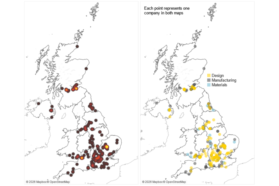
3.4 Location of dedicated semiconductor companies
Analysis of UK location data shows known clusters of semiconductor companies in Bristol, Cambridge, the North East of England, Northern Ireland, Scotland and South Wales. It also shows clusters in the North West, the Midlands and along the south coast of England.
Main manufacturing clusters are in Scotland, Wales and the North East. There are design clusters in and around London, particularly in Cambridge, and along arterial routes between London and Bristol, Oxford and Southampton.
Figure 3.6 – UK semiconductor clusters (dedicated companies)
Source: Companies House, Perspective Economics
4. Economic contribution
This section provides an updated analysis of the contribution that semiconductor activity makes to the UK economy.
4.1 Estimated revenue
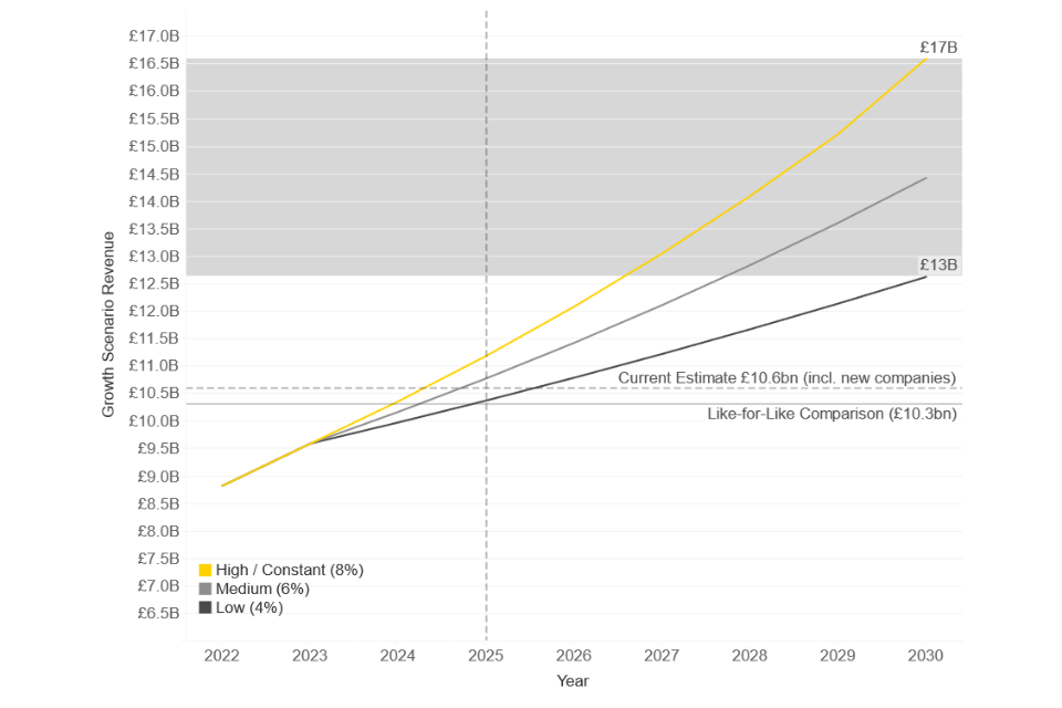
Since 2022 global semiconductor sales have soared, reaching a total of $796bn (£584bn) in 2025 (+39%)[footnote 13]. Estimated UK revenues among the same set of dedicated companies have grown by 7% from £9.6bn in 2022/23 to £10.3bn in 2024/25.
Improvements in the analytical tools and techniques available to identify and classify companies means that additional dedicated companies have been identified. If estimated UK revenues for those companies are also included, then total estimated revenues generated by dedicated semiconductor companies in the UK total £10.6bn (i.e. by 10%)[footnote 14].
Within this figure, dedicated companies involved in ChipStart, and other dedicated companies incorporated in 2024 and 2025 contribute £23m.
The baseline study used historic (10-year) revenue data for 40 dedicated semiconductor companies to calculate average compound annual growth rates. The resultant average growth rate of 8% was used as a basis to produce straight-line growth scenarios that assumed low growth (4%), moderate growth (6%) and constant or high growth (8%).
The current estimate of £10.6bn in sector revenues positions growth between the baseline low and moderate growth scenarios (Figure 4.1).
Figure 4.1 – Growth scenarios (dedicated company UK revenues)
Source: Perspective Economics
The 2024 study estimated that approximately 66% of UK revenues were generated by large companies. Based on the latest available data, the large company share of revenues has increased to approximately 75%. Revenue per employee ranges from £240k among micro companies (baseline = £225k) to £675k among large companies (baseline = £750k).
Analysis of estimated UK revenues by headquarters location shows a 50/50 split between UK headquartered companies, and companies headquartered internationally – consistent with the baseline study. Table 4.1 provides a breakdown of estimated UK revenues by company size and headquarters location.
Table 4.1 – Revenue by HQ location and size
| Estimated size | Intl HQ (£m) | Intl HQ | UK HQ (£m) | UK HQ |
|---|---|---|---|---|
| Large | 3,378 | 70.7% | 4,217 | 79.0% |
| Medium | 1,370 | 25.6% | 584 | 10.9% |
| Small | 183 | 3.4% | 436 | 8.2% |
| Micro | 16 | 0.3% | 104 | 1.9% |
| Total | 5,347 | 100% | 5,341 | 100% |
Source: Perspective Economics
The split in revenues across high-level supply chain categories (design, manufacturing and materials) are also broadly consistent with the baseline study, with design accounting for 79% of revenues (driven by a small number of very large design firms) and materials and manufacturing accounting for 17% (baseline = 85% and 15% respectively).
Future growth
Responses to the baseline survey of semiconductor industry representatives returned very positive expectations for future growth. At that stage, 90% of respondents (n=59) expected to see some level of business growth in the short-term (3 years). According to this year’s survey data, growth projections continue to be positive, with 83% of respondents (n=54) expect their UK semiconductor business to experience growth over the next three years[footnote 15]. Almost half of all respondents this year (47%) expect rapid growth of more than 20% per annum, compared to 38% in 2024.
As with the 2024 study, growth sentiment among design-oriented businesses tended to be more optimistic than among manufacturing or materials businesses. 57% of design-oriented businesses expect to see rapid growth in the next 3 years, compared to 35% of manufacturing businesses and 43% of materials businesses. Overall, however, growth sentiment among both manufacturing and materials businesses is also overwhelmingly positive, with approximately three quarters of respondents in both industry segments expecting to see business growth in the next 3 years.
When asked to identify significant barriers to business growth in the next 3 years. Talent availability is the most frequently cited growth barrier among design companies, appearing in approximately two thirds of responses – consistent with context set out in strategic reports filed with Companies House. Qualitative survey data also suggests that the concern is not only graduate supply but also challenges with finding experienced engineers at senior level, particularly in digital and mixed signal design. Respondents continue to cite Brexit as a compounding factor, suggesting that the UK is a less attractive proposition post-Brexit than other EU countries for international talent.
Access to capital was cited as another barrier to growth by respondents from different industry segments. Design companies, particularly early-stage and fabless businesses, reported difficulty securing growth equity and grant funding for hardware focused businesses. Lack of access to growth capital is also likely to be a contributing factor to broader structural concerns raised in qualitative survey responses that ‘success’ in UK fabless semiconductor endeavours tends to result in acquisition rather than sustained independent scaling, which several respondents describe as undermining long-term depth in the sector. Manufacturing companies cited scale-up capital as the primary growth constraint, with several respondents noting that government support is concentrated in R&D rather than more capital-intensive scale-up of production.
Lastly, UK operating costs, particularly energy costs, were a recurring theme among manufacturing respondents, some of whom suggested that current energy cost pressures are damaging global competitiveness, including with the Republic of Ireland.
4.2 Estimated employment
The baseline study estimated that dedicated UK semiconductor companies employed 15,000 people in the UK, and that UK headquartered companies accounted for more than 60% of that total (n=9,313).
Like-for-like comparison of estimated employment among companies included at both timepoints suggests that sector employment has grown by 9% to 16,350[footnote 16], with UK headquartered companies still accounting for 60% of this total.
Applying weighted employment multipliers to this direct employment base suggests that UK semiconductor activity supports a further 10,500 jobs through supply chain effects, and a further 5,700 in the wider economy. This brings the total number of jobs supported by the sector to 32,550.[footnote 17]
Employment by size and headquarters location
Among dedicated companies, around 66% of total employment is within large companies (up from 53% in the baseline study) and 23% of employment is within medium sized companies (down from 33% in the baseline study). This change is driven by a combination of employment growth among large companies such as Vishay, Arm, Renesas and KLA, shifts from medium to large size categories between the baseline and current study (e.g., Pragmatic Semiconductor) and comparatively modest changes in either direction among medium sized companies. Table 4.2 provides a summary of employment numbers and percentages within dedicated semiconductor companies of different sizes, according to whether they are headquartered in the UK or internationally. The data suggests that the share of employment among large companies, headquartered in both the UK and internationally, is greater than estimated in the baseline study.
Table 4.2 – Employment by HQ location and size
| Estimated size | Intl HQ | Intl HQ | UK HQ | UK HQ |
|---|---|---|---|---|
| Large | 4,099 | 57.2% | 6,636 | 72.4% |
| Medium | 2,412 | 33.6% | 1,359 | 14.8% |
| Small | 592 | 8.3% | 933 | 10.2% |
| Micro | 68 | 0.9% | 237 | 2.6% |
| Total | 7,171 | 100% | 9,165 | 100% |
Source: Companies House, Perspective Economics
Analysis of web data on technical employment within dedicated and diversified semiconductor companies suggests that 51% of those employed in dedicated companies work in technical roles. Survey responses suggest that 62% of employment is within technical roles, suggesting that the number of people employed in technical roles is between 8,500 and 10,000, higher than the 2024 estimate of 33% (5,000 employees).
Regional employment profile
Web data was used to estimate the number of dedicated semiconductor employees across regions. Results of the analysis suggest that the East of England, Scotland and the South East account for the highest proportions of dedicated semiconductor employees, and that the East of England, Wales and Scotland have among the highest concentrations of semiconductor employees relative to the concentration nationally[footnote 19].
Table 4.3 – Estimated employment across regions
| Region | Percentage of dedicated semiconductor employees | Location quotient |
|---|---|---|
| East of England | 20.6% | 2.29 |
| East Midlands | 3.6% | 0.52 |
| London | 12.6% | 0.72 |
| North East | 2.2% | 0.65 |
| North West | 8.5% | 0.78 |
| Northern Ireland | 1.9% | 0.74 |
| Scotland | 15.0% | 1.94 |
| South East | 11.9% | 0.88 |
| South West | 10.3% | 1.22 |
| Wales | 8.6% | 2.16 |
| West Midlands | 1.9% | 0.24 |
| Yorkshire and The Humber | 2.7% | 0.35 |
Source: Perspective Economics, Lightcast
4.3 Estimated gross value added
A like-for-like comparison of dedicated companies included across both datasets suggests that estimated gross value added (GVA) has fallen slightly from £7.4bn (2022/23 data) to £7.1bn (2024/25 data).
This is mainly due to reductions within one large internationally headquartered firm. Removing that one firm from both datasets reveals a positive underlying trend in which GVA has increased by 9%, from £5.8bn to £6.3bn.
Further, if newly identified dedicated companies are included in the GVA analysis, then dedicated sector GVA has increased from £6.6bn to £7.5bn (also by 9%).
5. Regional foundations, national capability
The UK semiconductor sector supports high-skilled, high-value jobs across every UK region. Activity across regions is led by business leaders and advocates with deep technical and sectoral knowledge. Every region brings distinct capabilities, from materials science and device physics through fabless design, IP, foundry, manufacturing, advanced packaging and process equipment. Regions connect through academic and industrial networks to create a national semiconductor capability that makes the UK an attractive global location for semiconductor research and development (across design and materials) and attracts substantive levels of foreign direct investment in manufacturing. The sub-sections below provide a summary of relative regional strengths. Full profiles are available in the report appendices.
5.1 East of England (Cambridge)
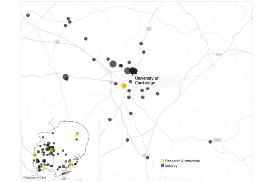
Cambridge hosts a globally leading semiconductor research and design ecosystem, with depth in fundamental semiconductor physics, world-leading GaN and advanced materials capability, and globally significant chip architecture expertise through Arm. The cluster is anchored by the University of Cambridge – the Cavendish Laboratory’s Semiconductor Physics Group, the Cambridge Centre for Gallium Nitride, and the new CASCADE Computer Architecture and Semiconductor Design Centre, founded by a £3.5m Arm donation in 2024.
Key capabilities include hafnium-oxide memristors for energy-efficient AI hardware, MOCVD GaN growth and porous nitrides (commercialised via Porotech), 2D materials work generating spin-outs such as Paragraf, CamGraPhIC and Molyon, and CASCADE/CHERI chip architecture leadership. Cambridge collaborates extensively across UK regions including as part of the Henry Royce Institute, via the UK-Ireland cross-border ANAM nanotube initiative, in Wales through IQE’s Cambridge-rooted supply relationships, and with Bristol and Warwick via REWIRE, Cambridge GaN Devices and Paragraf.
Business activity centres on design, IP and fabless semiconductor activity. Arm’s HQ anchors a base that includes Qualcomm, Imagination Technologies, MediaTek, AMD and Synaptics design centres.
5.2 London
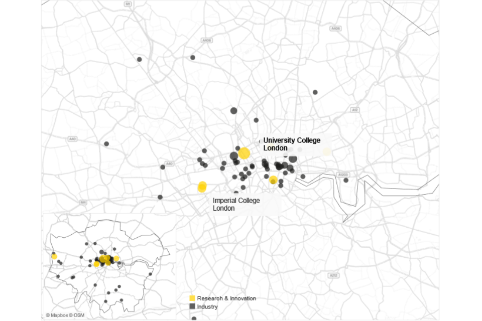
London is the strategic centre of the UK semiconductor sector, as the location for national coordination bodies, startup programmes and proximity to government and capital markets. The newly established UK Semiconductor Centre (UKSC) at the Institute of Physics convenes national policy, with team members distributed across the UK to support regional clusters.
Research is led by UCL and Imperial College London. UCL has unique national strength in neuromorphic computing, hosting the Neuroware IKC dedicated to its commercialization, alongside the London Centre for Nanotechnology. Imperial leads on MEMS, terahertz optics and single-atom silicon quantum electronics.
The Knowledge Quarter at King’s Cross offers proximity to Google, DeepMind, Meta and Advanced Research and Invention Agency (ARIA). Business activity focuses on fabless design, IP and research-led spin-outs, including Fractile, Olix, Allegro, Semtech and Nanoco.
5.3 North East
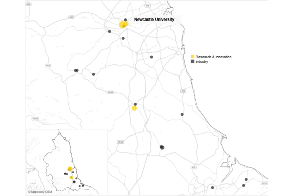
The North East is a business-led advanced electronics cluster focused on capabilities that go beyond conventional silicon to compound semiconductors, two-dimensional materials, polymer and organic materials, and hybrid approaches. The cluster is organised around the North East Advanced Material Electronics (NEAME) cluster body and grounded in long industrial heritage, with member companies spanning the full value chain from electronic materials manufacture through device development, fabless design and product integration.
Distinctive regional capabilities include compound semiconductor RF and millimetre-wave components, MEMS manufacturing, photonics for space and aerospace, and frontier flexible/organic and radiation detection electronics. Newcastle University’s research, hosted within the CHIMES’ IKC, focuses on next-generation integrated circuits.
Through CHIMES’ the cluster connects to joint leads Sheffield and Southampton, and to Manchester. The Compound Semiconductor Applications Catapult’s NETPark site links the North East to South Wales’ national compound semiconductor infrastructure, and Pragmatic Semiconductor’s North East operations tie the cluster to Cambridge’s flexible electronics ecosystem. Regional semiconductor companies include Filtronic, Coherent, INEX, Isocom, Tosoh Quartz, aXenic, Mignon, Nascent Semiconductor and EpiValence.
5.4 Northern Ireland
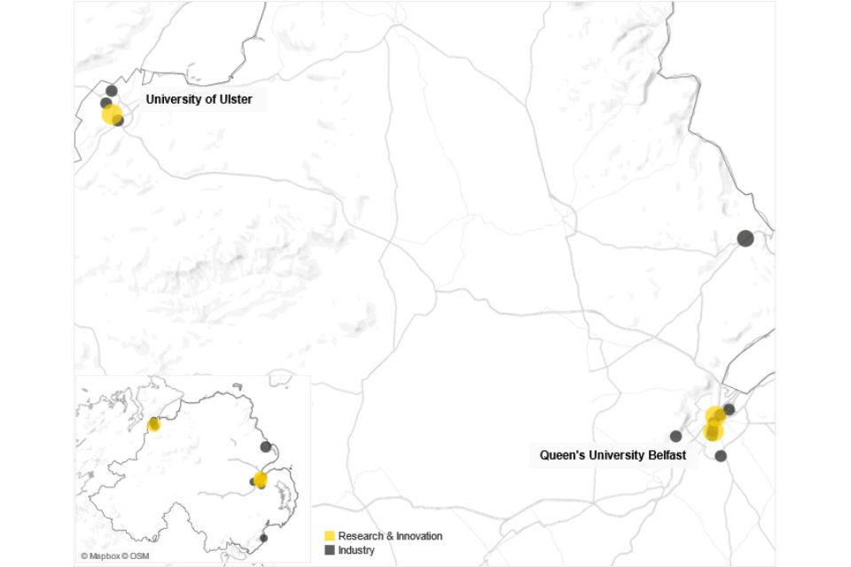
Northern Ireland is home to nationally influential hardware security research base. Regional capability is anchored by Seagate Technology – a global leader in mass-capacity data storage and lead partner within the £42m Smart Nano NI consortium. Smart Nano NI is also supported by Queen’s University Belfast, Ulster University, and the Queen’s Advanced Micro-Engineering Centre (QAMEC), with cluster coordination through the Northern Ireland Photonics Innovation Cluster (NIPIC).
Distinctive technical strengths include integrated photonics and nano-manufacturing, hardware security and secure-by-design research at Queen’s Centre for Secure Information Technologies, and novel materials work via Ulster’s involvement in the Cambridge-led Advanced Nanotube Application and Manufacturing Initiative (ANAM). The cross-border Semiconductor Photonics Education and Research (SPEAR) Centre acts as a UK–Ireland innovation hub.
Business activity is anchored by Seagate’s 20-acre advanced manufacturing plant – critical to the global heat-assisted magnetic recording head supply chain – and ICEMOS Technology (silicon-on-insulator and MEMS foundry). Specialist firms include Raptor Photonics, Wolfspeed, Arralis, Amphion Semiconductor, Brolis Photonics, AntennaWare, Silansys, and Causeway Sensors.
5.5 North West
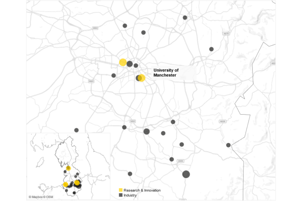
Manchester is home to an internationally significant semiconductor-adjacent materials research ecosystem. Its relevance to semiconductors is concentrated upstream in fundamental materials science, characterisation infrastructure and national coordination underpinning the UK’s ability to move beyond silicon.
Regional capability is anchored by the University of Manchester through the National Graphene Institute (NGI), the Graphene Engineering Innovation Centre (GEIC), and the Henry Royce Institute, the UK’s national institute for advanced materials which connects to Sheffield, Leeds, Liverpool, Cambridge, Oxford, and Imperial College London. Manchester is also a CHIMES’ IKC member, linking it to Newcastle, Sheffield and Southampton. Industrial translation includes but is not limited to GEIC partnerships with BAE Systems, Honda, Haydale, Smart IR, Levidian and the National Physical Laboratory, alongside the Royce’s ‘Atoms to Devices’ programme spanning Cambridge, Imperial, Leeds and Manchester.
Regional businesses include but are not limited to Nexperia, Graphcore, Intel, Texas Instruments, and Diodes.
5.6 Scotland (Edinburgh)
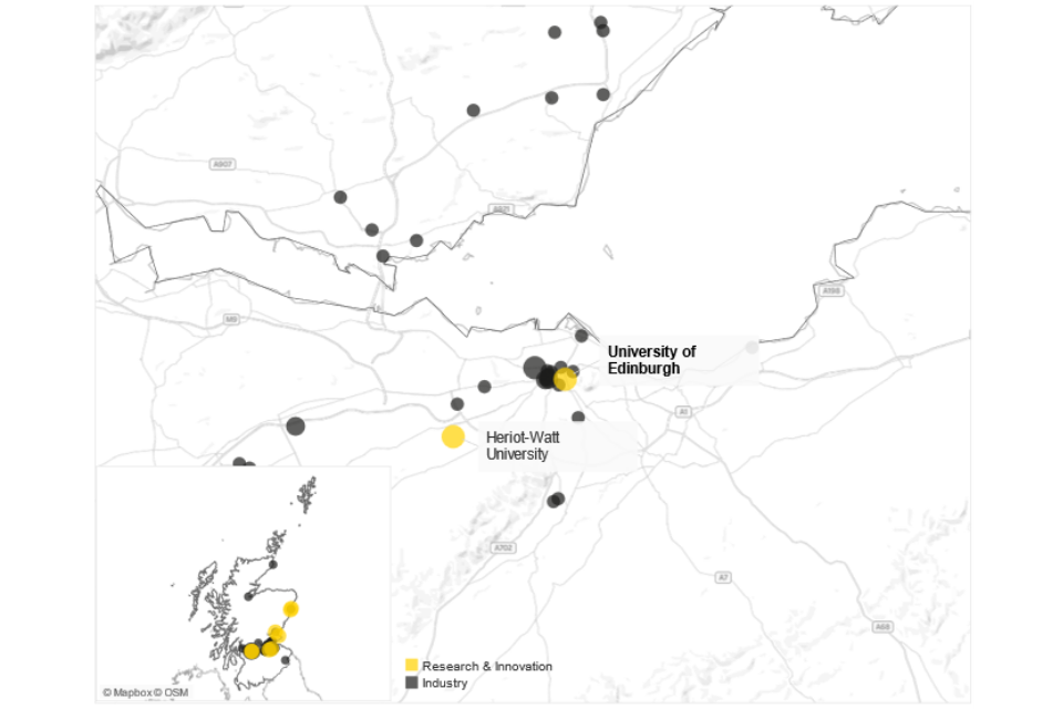
Edinburgh is a research-and-fabrication centre which enables the integration of physical fabrication capability, emerging device science and AI-hardware co-design. The Scottish Microelectronics Centre (SMC) provides an industrial-standard 250m² cleanroom delivering lithography, dry etching, metallisation, deposition, parametric testing and characterisation on wafers up to 200mm, supporting direct process transfer to industry.
The Centre for Electronics Frontiers (CEF) at the University of Edinburgh maintains relationships with over one hundred global companies, leading research on memristors, neuromorphic architectures, adiabatic computing, and silicon demonstrators.
Edinburgh anchors national-scale collaboration through the AI for Productive Research & Innovation in eLectronics (APRIL) hub, which links 20 universities and 30+ industry partners across five innovation pillars in an effort to apply AI systematically to the electronics supply chain from materials discovery through verification and testing.
Business activity centres on a cohort of dedicated semiconductor firms including but not limited to Shin-Etsu, Cirrus Logic, Semefab, Clas-SiC, Sivers Semiconductors, Dukosi and Alter Technology.
5.7 Scotland (Glasgow)
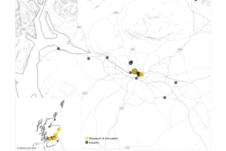
Glasgow hosts one of the UK’s most substantial and historically rooted concentrations of semiconductor and photonics technology capability. The Scottish photonics sector – largely concentrated around Glasgow – generates over £1.2 billion in annual turnover, employs approximately 6,400 people, and exports 97% of its output. Photonics Scotland coordinates a community of over 50 companies alongside a globally recognised academic base at the Universities of Glasgow and Strathclyde (Institute of Photonics and the co-located Fraunhofer Centre for Applied Photonics).
Distinctive capabilities include the University of Glasgow’s ANALOGUE advanced semiconductor packaging facility; silicon-compatible quantum-enabled sensing and mid-infrared photonics; GaN micro-LED leadership at Strathclyde’s Institute of Photonics; and applied laser/photonic technology at Fraunhofer Centre for Applied Photonics (CAP).
Glasgow co-hosts the CORNERSTONE silicon photonics foundry with Southampton and STFC, partners the Integrated Quantum Network and QuantIC consortia, leads QT Assemble with Fraunhofer IAF, and anchors the TITAN national telecommunications hub.
Business activity is weighted towards photonics, quantum and design. Regional companies include but are not limited to FTDI, Coherent, Skylark Lasers, Ichor Systems, Retronix Semiconductor and Synaptec.
5.8 South East (Southampton)
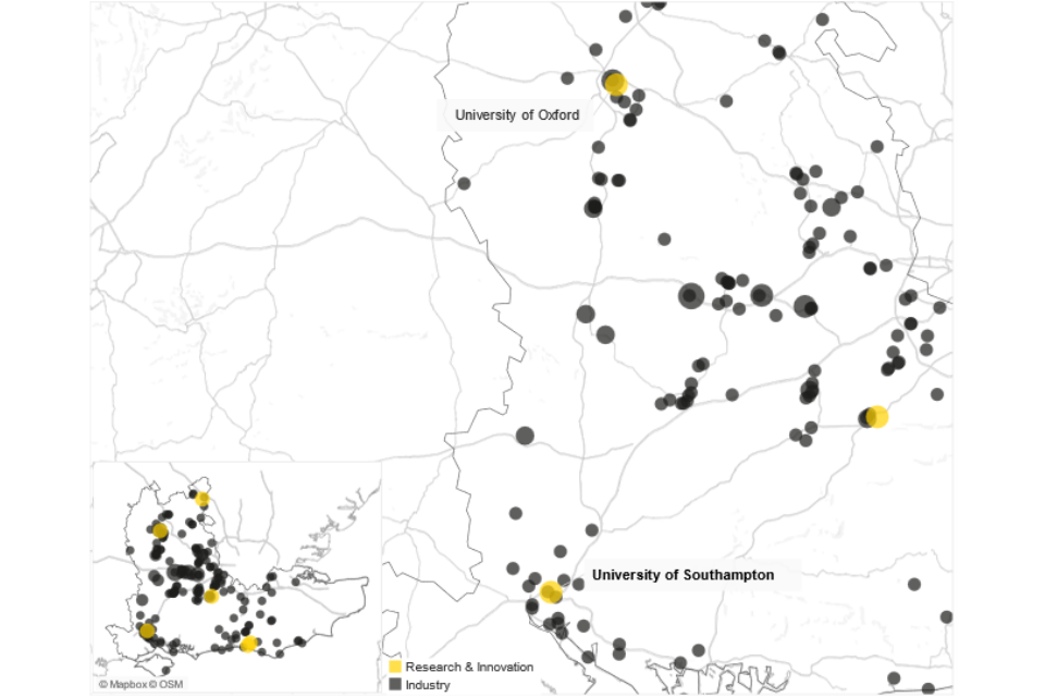
Southampton hosts one of the UK’s most strategically significant and infrastructure-rich semiconductor research. It is home to internationally-leading silicon photonics capability, including uniquely advanced fabrication infrastructure, and is a key partner in multiple national programmes. Regional capability is anchored by the University of Southampton’s Optoelectronics Research Centre, the Zepler Institute, and the Southampton Nanofabrication Centre.
The CORNERSTONE silicon photonics foundry, operated jointly with the University of Glasgow and STFC, provides national rapid-prototyping capability.
Distinctive research strands span silicon photonics foundry services, advanced nanofabrication, nonlinear semiconductor photonics for wavelength conversion and entangled photon pair generation, and systems-level translation of fundamental research to foundry prototyping.
Southampton jointly leads the CHIMES’ IKC with Sheffield, jointly leads the EXPRESS programme with Warwick (focused on growing next-generation semiconductor materials), partners with Sheffield’s National Epitaxy Facility, contributes to the QuantIC consortium, and partners Glasgow’s Fraunhofer CAP-led QT Assemble project.
The South East business base is weighted towards but not limited to multinational design and IDM activity, including companies such as Synopsys, Cadence, Broadcom, Renesas, NXP, Micron, STMicroelectronics and Microchip Technology.
5.9 South West (Bristol)
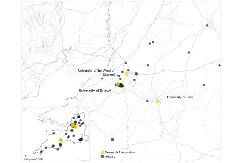
Bristol is emerging as a centre for semiconductor-related research and innovation. The cluster has distinctive capabilities in materials science, device design, RF and power electronics research, and characterisation infrastructure for translating novel materials into deployable devices. Three research strands are prominent including: next-generation power semiconductors through REWIRE; RF and 6G work, including a May 2025 Nature Electronics paper on GaN amplifiers; and advanced materials characterisation.
Bristol is connected to Warwick and Cambridge through the REWIRE IKC, which is supported by a dense industrial partner network.
Business activity spans power, RF and photonics, including but not limited to Plessey Semiconductors, Infineon, Effect Photonics, XMOS, Blu Wireless, Swindon Silicon Systems, Codasip and Lew Techniques.
5.10 Wales (South Wales)
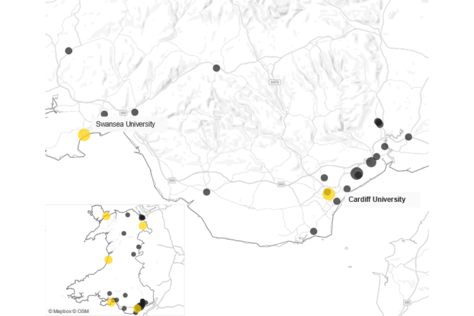
South Wales hosts one of the UK’s most clearly defined and institutionally mature semiconductor clusters – internationally recognised as the world’s first compound semiconductor cluster. Grown from a 2015 collective vision, it is now a strategic national asset with deep alignment between universities, industry, public sector and global investors. Over the past decade more than £850 million has been invested in research, pilot fabrication, manufacturing and innovation across a 70-mile Chepstow–Swansea corridor.
The region provides a near-complete vertical supply chain spanning epitaxial growth, prototyping, wafer manufacturing, device fabrication, advanced packaging, module integration and process tool / metrology equipment. Research activity takes place across South Wales, including within the Compound Semiconductor Centre, Cardiff’s Institute for Compound Semiconductors, and Swansea University’s £29.9m Centre for Integrative Semiconductor Materials (CISM), which houses the MOCVD Centre, the UK’s only pilot line for Silicon Carbide (SiC) power components, and is the UK’s only translational pilot fab designed on industrial principles.
Business activity centres on volume manufacturing and supply chain depth, including but not limited to the ‘core 4’ of IQE, Vishay Newport, KLA, and Microchip Technology, as well as Photronics, Novomorphic, Thalia, Irresistible Materials, Kubos, Ffotoneg and Space Forge.
5.11 West Midlands (Warwick)
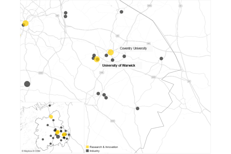
Warwick hosts a focused and technically ambitious semiconductor research programme concentrated at the University of Warwick, focused on deep group-IV semiconductor materials physics, with a strong emphasis on silicon-compatible quantum and next-generation electronic materials, and shared nanofabrication infrastructure. Regional capability is anchored by the Semiconductors Research Group within the Department of Physics, the Nano Fabrication Research Technology Platform (an ISO class 6 cleanroom spanning deposition, lithography, etching, thermal processing and metrology), and the EXPRESS programme.
Distinctive technical capabilities include scalable electrodeposition routes, group-IV materials physics, the EPSRC Centre for Doctoral Training in Diamond Science and Technology, the Theoretical Physics Group, and Warwick Manufacturing Group’s scale-up engineering.
Warwick is connected nationally to Southampton, Bristol and Cambridge through the EXPRESS and REWIRE initiatives, with industrial connections made via the Warwick Innovation District.
Business activity includes but is not limited to Active Silicon, Solsta, Transys Electronics, Advanced Epi, and Kopin UK.
5.12 Yorkshire and Humber (Sheffield, Leeds)
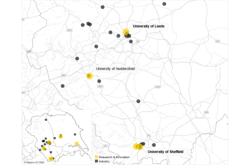
Sheffield has developed a distinctive semiconductor research and innovation base, combining national research infrastructure, a heterogeneous integration design centre, and an established advanced manufacturing capability – a combination that has positioned the region at the centre of the recently announced £50m Defence Growth Deal for South Yorkshire. The University of Sheffield anchors this base, with capability extending across the wider Yorkshire and Humber region through the School of Electrical and Electronic Engineering and the Semiconductor Materials and Devices group.
Sheffield’s semiconductor strengths span four complementary strands, including III-V compound semiconductor materials and devices, heterogeneous microelectronic integration system design through CHIMES’ IKC, millimetre-wave characterisation via the National Millimetre Wave Facility, and photonics, optoelectronics and quantum devices. The Bragg Centre at the University of Leeds adds distinctive fabrication strengths enabling electron-beam lithography and supporting bionanotechnology, microfluidics prototyping, and soft-matter device processing, positioning Leeds as a key partner for hybrid and unconventional device fabrication. Together these strands provide capability from epitaxial materials growth through heterogeneous system design to characterisation and test, with a route into production engineering through the University of Sheffield Advanced Manufacturing Research Centre (AMRC). AMRC’s Digital team supports semiconductor packaging, heterogeneous integration assembly and defence supply-chain resilience via digital twins, AI-driven process optimisation and digital factory architectures, drawing on an industrial membership network that includes BAE Systems, Rolls-Royce and Boeing.
Sheffield is a key collaboration node: CHIMES’ is jointly led with Southampton and has Newcastle and Manchester as members, the National Epitaxy Facility serves UCL, Cambridge and the wider UK research base, and Leeds’ Bragg Centre operates within the Royce hub-and-spoke model. Business activity comprises Arm and EnSilica design centres in Sheffield, Optalysys in Leeds, Aegiq, Phlux Technology, Pixel-Flo and Sitehop. Research-linked firms includes Iceotope Technologies, Diamond Microwave, Apitronix Semiconductor in Huddersfield, Analogic in Halifax and Ngenics in York.
5.13 Role of regions in UK semiconductor activity
As highlighted in the baseline study, Arm accounted, and still accounts for a significant proportion of both total revenue, and total employment among dedicated, UK headquartered semiconductor companies. With its headquarters in Cambridge, Arm continues to make the East of England a focal point of semiconductor sector activity in the UK.
To better understand the geographic composition of semiconductor activity among other companies, the study looked specifically at a subset of dedicated UK headquartered companies excluding Arm[footnote 20]. Analysis of this subset of companies emphasises the significance of regions outside London and the South East to the UK’s semiconductor sector (Table 5.4). For example, within this subset, while Wales is home to less than 10% of dedicated, UK headquartered companies, it accounts for 11% of employment and 24% of revenues. Scotland accounts for 19% revenues and the South West accounts for 13% of employment.
Table 5.4 – Role of regions in UK semiconductor activity
| Region | % firms | % revenue | % employment |
|---|---|---|---|
| East of England | 26 | 27 | 26 |
| London | 14 | 5 | 16 |
| Scotland | 15 | 19 | 19 |
| South East | 25 | 16 | 15 |
| South West | 13 | 9 | 13 |
| Wales | 7 | 24 | 11 |
Source: Perspective Economics
6. Sector dynamism and maturity
This section provides insights regarding dynamism within, and maturity of the UK semiconductor sector. It draws on a combination of desk research, quantitative analysis of secondary data sources and consultations with 38 stakeholders from across the semiconductor ecosystem. Topics include perceived UK strengths, recent research and innovation activity, UK strategy and policy, investment, skills and future opportunities.
6.1 Perceived UK strengths
A series of UKSC briefing reports produced as part of the Centre’s roadshow initiative[footnote 21] pointed to UK semiconductor strengths such as: design and IP (Cambridge), compound semiconductors (especially the South Wales cluster), integrated photonics (Southampton / Glasgow / Northern Ireland), advanced packaging, and neuromorphic computing. Consultation with 38 semiconductor sector stakeholders spanning industry, academia and policy spheres similarly pointed to similar strengths, including:
- i) chip design and IP, anchored by Arm, wider design ecosystems including Imagination, Dialog (now Renesas) and with extensive engineering expertise throughout the UK
- ii) Compound Semiconductors and Photonics, with South Wales, Glasgow and Southampton routinely cited
- iii) the UK’s academic research base, consistently highlighted as a key asset
- iv) power electronics, particularly in compound forms and for high-voltage applications
- v) a less well recognised strength in specialist consumables and equipment manufacturing
These strengths are seen to be the result of the university research base, accumulated tacit know-how (often inherited from now-departed anchor companies), and cluster effects.
I think we’ve got great technologists. I think that’s a primary skill, we’re very creative, very innovative.
Increasingly connected ecosystem
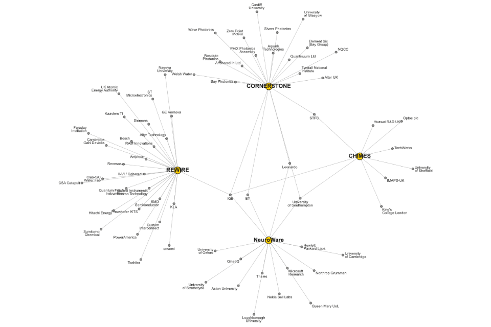
Public funding for the UK Semiconductor Centre, and university-led semiconductor initiatives has been allocated in an effort to further advance and leverage UK strengths via a central focal point (UKSC) and four innovation and knowledge centres (IKCs). These have broadly been seen as positive developments since 2024.
Table 6.1 – Publicly funded research interventions
| Intervention | Relevance to UK strengths |
|---|---|
| REWIRE IKC – wide/ultra-wide bandgap power semiconductors (Bristol, Warwick, Cambridge) | The UK is seen as having world-class capability in next-generation power semiconductors across silicon carbide (SiC), gallium nitride (GaN), and the emerging gallium oxide (Ga₂O₃). Bristol hosts Europe’s first Ga₂O₃ MOCVD machine and has demonstrated 4kV+ breakdown voltage devices. Warwick operates one of the UK’s only industrial SiC CVD reactors. Research spans the full device pipeline from epitaxial growth through to packaged prototypes, >30 partners including Bosch, Toshiba, and ST Microelectronics. Applications target net zero: EV charging, renewable energy, smart grids, extreme environment electronics. |
| CORNERSTONE (C-PIC) IKC – silicon photonics (Southampton, Glasgow, STFC) | Cornerstone provides an open-source, licence-free silicon photonics foundry offering seven technology platforms from near-infrared to visible wavelengths on 8-inch wafers. Founded in 2014, housed in Southampton’s £120M cleanroom, CORNERSTONE serves collaborators in 20+ countries through regular multi-project wafer runs. Strengths include custom/non-standard fabrication increasingly unavailable from commercial foundries. Applications span telecoms into quantum technologies, AI hardware, environmental sensing, and LiDAR. |
| CHIMES IKC – heterogeneous integration system design (Sheffield, Southampton + 10 academic partners) | The Centre for Heterogeneous Integrated MicroElectronic and Semiconductor Systems (CHIMES) provides national capability in heterogeneous integration i.e., combining different semiconductor chiplets into unified high-performance systems. CHIMES focuses on creating a shared ‘Design Commons’ of reusable architectures, workflows, and design tools to lower barriers for UK companies. A distinctive strength is the secure-by-design approach, building Cambridge’s CHERI architecture and Arm’s Morello prototype. The centre targets power management, wireless communications (5G/6G), photonics, and sensors, and aims to convert UK research IP into physical ‘Hard-IP’ chiplets. |
| NeuroWare IKC – neuromorphic computing (UCL, Cambridge, Oxford, Manchester, Strathclyde, Sheffield, Imperial College London, King’s College London) | NeuroWare is a new multi-institution Innovation and Knowledge Centre (IKC) dedicated to advancing neuromorphic computing – brain-inspired computing architectures – through academic and industry collaboration. Led by University College London (UCL Electronic & Electrical Engineering, with involvement from STEaPP), the consortium also includes the universities of Cambridge, Oxford, Manchester, Strathclyde, Sheffield, Imperial College London, King’s College London, and the National Physical Laboratory (NPL). The IKC involves around 30 industrial partners, with named anchors being Arm, Intel, Microsoft, HP, Samsung, and the Tyndall Institute, plus start-up networks and VC investors. |
Source: Perspective Economics, IKC websites
Collation of publicly available data on networks being established across the four IKCs points to their strategic relevance. Each IKC is engaged with large global semiconductor companies, and the IKCs are also connecting businesses and academic institutions across the UK semiconductor ecosystem. Figure 6.1 below provides an illustration of evolving IKC networks, which total 66 unique connections across industry and academia.
Figure 6.1 – IKC networks
Source: Perspective Economics, IKC websites
Research and innovation funding
The 2024 study estimated that between 2006 (beginning of structured UKRI funding records) and 2023, semiconductor related research and innovation had received £1.4bn in public investment. By the end of 2025 research and innovation funding for semiconductor activity is estimated to be £1.8bn[footnote 22]. Between 2024 and 2025 five high-level semiconductor topics have secured just under 60% of new funding allocations, including compound materials (14%), compound semiconductor manufacturing (13%), 3D packaging and integration (12%), photonic integrated circuit design and fabrication (11%) and memory (7%)[footnote 23].
One of the major advantages that the UK semiconductor industry has is [the] knowledge and industry expertise around compounds. It’s really something that’s quite unique.
Figure 6.2 – Recent funding focus
| Semi-conductor topics | New funding allocations |
|---|---|
| Compound materials | 14.0% |
| Compound semiconductor manufacturing | 12.6% |
| 3D packaging and integration | 11.8% |
| Photonic IC design and fabrication | 11.0% |
| Memory | 7.4% |
Source: Perspective Economics, UKRI (incl. SIPF and RPIF)
As part of horizon scanning research conducted to inform this iteration of the study, workshop participants noted that memory technology is an increasingly important part of the AI compute opportunity, and that it should garner greater recognition as a potential UK capability opportunity.
UK memory opportunity
Memory technology makes up an estimated 28% of the $1 trillion semiconductor market (WSTS Autumn 2025 Forecast). Despite early forays into this market in the 1970s with INMOS, the UK has no remaining sovereign capability, which now all resides in Asia and is subject to near insurmountable barriers to entry. However, there is global recognition that the memory market is ripe for disruption given the need for lower power to support all areas of application along with the growth of novel architectures e.g. non-Von Neumann, neuromorphic and the convergence of memory with processing as well as supporting quantum computing. Since 2019, semiconductor companies have applied for and / or been granted over 1 million patents concerning semiconductor memory technologies. Horizon scanning research conducted to inform this study has highlighted a) that frontier semiconductor memory technology represents a significant opportunity for the UK and b) that leading-edge UK companies that epitomize this opportunity are now facing scale-up barriers that could see them pursue operations internationally aligned to funding opportunities, risking a repeat of the UK’s INMOS experience.
Intellectual property
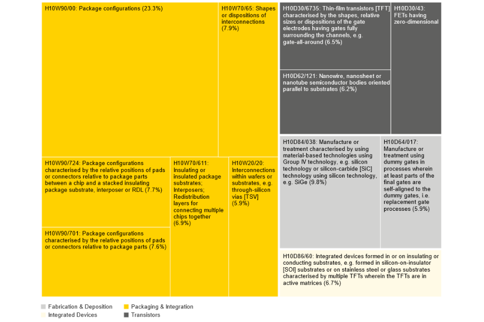
In the baseline study, a search for data on patents either applied for or granted between 2018 and 2023 within the US, the UK or Europe returned a total of 525,000 patent records[footnote 24]. At that stage, 81% of patent records applied to the US, 17% applied to Europe and 2% applied to the UK. Re-running the same patent query with a cut off date of 31st December 2025 returns a total of 597,100 patent records – an almost 14% increase within two years. 84% of those apply to the United States, 14% apply to Europe and 2% apply to the UK. In absolute terms, the number of US patents applied for or granted since the baseline study has increased by 18%. Within the last two years, US applications have been driven by TSMC, Samsung, BOE, LG, Intel, Applied Materials, Tokyo Electron and Micron Technology. European patent activity has been led by Samsung, BOE, the Atomic Energy Commission, Intel, LG, Huawei, Sony and Applied Materials. UK activity has been led by LG, BOE, IBM, Cirrus Logic, Skyworks Solutions, Sumitomo Chemicals and UK headquartered companies Pragmatic Semiconductor and Paragraf. Over the same period, Arm has had 820 patents (all US oriented) either applied for or granted under a range of physics classifications including processor architectures, processor configuration, general purpose rendering architectures, memory management and latency reduction. Figure 6.3 shows the technological focus of patent activity between 2024 and 2025, 60% of which relates to packaging and integration.
Figure 6.3 – Focus of patent activity
Source: Perspective Economics, Lens.org
To better understand UK involvement in patent activity, the study applied the same approach used to identify and classify semiconductor research projects, to US patents granted between 2020 and 2025 that have at least one UK-located inventor or assignee. A total of 1,139 of the 56,980 UK-related US patents (2.0%) were considered to be semiconductor-related. Analysis of those patents across the supply chain provides some insight into technical UK expertise:
-
Pure design (497 patents, 44%): including EDA software, formal verification and design-flow tooling, plus circuit- and IP-level designs for digital ICs, analog ICs, memory, RF/microwave and quantum devices. This category is dominated by Arm (>100 patents across memory, digital and RF/microwave), Imagination Technologies, Pulsic, Graphcore, Dialog Semiconductor UK and a tail of EDA spinouts.
-
Device engineering (336 patents, 29%): covering patents on the physical structure of devices themselves, mostly optoelectronics, transistors and diodes. This tier includes patents across the design / manufacturing boundary i.e., the patent claims a device structure, but the structure is tied to a specific fabrication process. Most of this category is filed by fabless device companies that outsource fabrication, such as Rockley Photonics, Cambridge GaN Devices, ORCA Computing, and Dynex Semiconductor.
-
Manufacturing and supporting infrastructure (306 patents, 27%): including wafer fabrication and process steps (across etch, deposition, lithography, integration, doping, isolation and thermal), packaging and assembly, materials, metrology and inspection, and fab equipment. This category includes specialist process companies such as KLA (under SPTS), IQE and Edwards.
Analysis of UK-US patents granted most recently (in either 2024 or 2025) suggests that the focus of UK input has shifted from pure design towards device engineering (see Table 6.2 – note totals sum to 99% because a small number of patents had insufficient information to be classified in both periods).
Table 6.2 – Focus of recent patent activity (2024 – 2025)
| Supply-chain component | 2020–23 share | 2024–25 share | Change (pp) |
|---|---|---|---|
| Pure design | 47% | 36% | -11 |
| Device engineering | 27% | 37% | +10 |
| Manufacturing and supporting infrastructure | 26% | 26% | – |
| Source: PatentsView, Perspective Economics | n=846 (2020 – 2023), n=293 (2024 – 2025) |
Table 6.3 – UK patent assignees by granted patents (2024 – 2025)
| Assignee | Focus |
|---|---|
| Rockley Photonics Limited | Silicon-photonics device engineering |
| Arm Limited | Memory and on-chip system design |
| STMicroelectronics R&D UK Limited | Optoelectronics, sensing, packaging |
| Imagination Technologies Limited | Digital IC design, formal verification |
| Cambridge GaN Devices Limited | GaN power transistors |
| KLA (SPTS) | Etch and deposition equipment |
| Flexenable Technology Limited | Flexible electronics materials |
| Flusso Limited | MEMS flow-sensor ICs |
| Graphcore Limited | 3D packaging, AI accelerators |
| Pragmatic Semiconductor Limited | Flexible thin-film ICs |
Source: PatentsView, Perspective Economics
6.2 Investment
Across the 190 companies included in both the baseline and current study, the value of grants and fundraising has increased by 16% from £1.5bn to £1.73bn. Ten companies account for 75% of new grant and fundraising activity – seven are design companies, two are materials companies and one is a manufacturing company.
Newly identified dedicated companies have secured £400m in grants and fundraising, 84% of which has been secured by design-oriented companies, and almost 70% of which has been secured by companies at seed or venture stages, including companies like Fractile and Olix Computing. Companies with registered offices in the East of England account for 46% of grants and fundraising among newly identified companies, London accounts for 26% and the South East accounts for 15%.
Foreign direct investment
Between 2003 and the end of 2025 there have been a total of 142 inward investment projects into the UK – 13 additional projects since the baseline study totalling an estimated $600m (£446m) in capital investment (+21%). This includes substantive investments by Vishay, KLA, Ion Beam Services and Cadence Design Systems. Over 80% of the estimated inward capital investment is from the US, and 90% has been from manufacturing companies.
Intra-company investment
Analysis of Companies House filings for more than 40 of the UK’s most significant dedicated semiconductor companies highlights less obvious forms of parent-company investments in the form of (among other mechanisms) parent equity injections, intercompany debt conversions and multi-year intercompany loan facilities. Across the filings analysed, this type of investment amounts to approximately £0.5bn of one-off equity events in a single year. Examples include but may not be limited to Vishay, Quantinuum / Honeywell, Graphcore, and Plessey. The total stock of intercompany funding that sits behind the sector is larger again, estimated to be net inward funding into the UK of £2.1bn, which serves as an indicator of foreign-parent commitment to UK semiconductor capability.
6.3 Perceived gaps, growth barriers and risks
Beyond the fundraising points raised above, consultation with sector stakeholders identified four other recurring themes in discussions about current gaps and growth barriers. These included access to finance for manufacturing capex and market distorting subsidies being offered abroad, skills (particularly mid-career and technician roles), commercially-competitive incentive packages, and coordination and clarity of strategy.
Regarding support for manufacturing activity, consultees perceived that UK companies are in a less competitive position due to comparatively high levels of subsidies being provided by governments in other countries, and challenges accessing finance to support high capital expenditure more generally. Consultees suggested that equivalent levels of subsidy and improved access to finance for large scale capital expenditure could strengthen the UK’s domestic manufacturing base.
A range of skills gaps were cited across consultations including, at the base of the skills pyramid, a simple lack of awareness of job opportunities in the semiconductor industry, to future workforce gaps caused by retirement of the current workforce, and specific gaps including a lack of technicians and insufficient numbers of equipment engineers. This is in keeping with findings from the UK Semiconductor Workforce Study (2025)[footnote 25].
Thirdly, several consultees emphasised the international nature of the semiconductor workforce, and the fact that UK businesses are required to compete for talent with companies in other jurisdictions where incentives are available to assist (or de-risk) the cost of employment. Again, Ireland was cited as a comparator with consultees suggesting that grants can help reduce the cost of expanding a semiconductor team by up to 25%[footnote 26].
Lastly, consultees reiterated the call for greater coordination and strategic clarity across the sector. In particular, consultees considered that more granularity regarding objectives, targets and actions over a 3 to 5-year timeframe would be beneficial, and that continued effort is required to reduce perceived fragmentation across the industry.
Consultees agreed that universities are foundational to UK semiconductor activity, with academia positioned as one of the key routes to de-risking innovation. However, consultees also highlighted some scope to improve productivity within translational research and innovation facilities. For example, cleanrooms could be operational more often, and it may be beneficial for capex funding to extend to operating costs or staffing.
When asked about opportunities to further leverage UK semiconductor sector opportunities, consultees highlighted workforce retention, preventing capital-driven offshoring of successful UK firms, alleviating structural subsidy disadvantages, mitigating the risk of concentrated packaging and materials supply in Asia and increasing the translation of internationally-leading research outputs to industrial scale.
Production capacity
Survey respondents involved in semiconductor manufacturing were asked to provide information regarding current and potential future production capacity. While limited detail can be provided here due to commercial sensitivities and risk of disclosure, analysis of production data returned two key findings; i) that in the absence of labour constraints production among the businesses that responded to the survey could more than double from current levels (in the order of tens of thousands of wafer starts per month), and ii) latent capacity for growth exists, in the form of 18% under / unutilised cleanroom floorspace.
6.4 Horizon scanning
This study gathered views from sector stakeholders regarding future opportunities and the UK’s role within them via a combination of one-to-one consultations, a horizon scanning workshop, and follow-up inputs from workshop participants. Six themes consistently emerged across these research strands.
-
AI is the dominant driver of new opportunities, with greatest UK opportunity in the supporting parts of the AI compute stack, such as inference chips, edge devices, photonic interconnect, advanced packaging, power electronics, and novel architectures – where the UK can compete on capability rather than capital intensity. Workshop participants similarly identified AI-enabled chip design and photonic chips as the two top technology priorities.
-
Compound semiconductors as a distinct UK strength, with applications spanning telecoms, datacoms, defence, automotive, renewable energy, and quantum systems, would benefit from a coordinated ten-year roadmap for wide-bandgap design, materials, devices, packaging, and integration, aligned to UK end markets in automotive, aerospace, defence, grid, and industrial applications, supported by a supply chain adoption programme that lowers barriers to existing open facilities and strengthens connectivity between academia and industry.
-
Photonics as a near-term opportunity where the UK has some differentiation, building on existing silicon photonics fabrication capability and a deep compound semiconductor ecosystem. Consultees referred to photonic ICs for data communications as part of the second wave of AI-driven demand, while workshop participants proposed a dedicated photonics pilot line and scale-up facility to bridge the gap from UK research to production, including low-volume defence manufacturing.
-
Heterogeneous integration and advanced packaging were often cited across all strands as critical enabling capabilities. Consultees flagged advanced packaging and chiplets as part of the AI-driven demand opportunity, while workshop participants gave heterogeneous integration and verification more emphasis as a critical enabling technology in its own right. All horizon scanning inputs treat the ability to combine diverse chip technologies into working systems as a distinct UK opportunity.
-
Pilot and translational infrastructure as a key commercialisation enabler. Consultees called for long-term Fraunhofer (Germany), Tyndall (Ireland), and DTU (Technical University of Denmark)-style operating support for RD&I infrastructure, which provide shared, capital-intensive equipment (cleanrooms, pilot lines and prototyping fabs) that individual firms, particularly SMEs and start-ups cannot afford to build or maintain alone. European facilities were cited as good practice references for commercially accessible, around-the-clock operations. Workshop participants independently proposed a Fraunhofer-lite design and integration centre and a photonics pilot line, and identified national infrastructure for chip design (cloud compute resources, EDA access, extended ChipStart-style programmes, and alignment with European platforms such as IMEC) as currently insufficient. Follow-up input noted the need for formal mechanisms to fund researcher and industry access to existing capabilities.
-
Energy and power emerged as a cross-cutting strategic opportunity. Consultees identified AI-driven demand for power, wide and ultra-wide bandgap power electronics (SiC, GaN, gallium oxide), and the wider infrastructure of power racks and delivery as recurring opportunities aligned to electrification, defence, space, and renewable energy. Workshop participants described the data centre ‘power crunch’ as a full-stack, national-scale problem requiring a coordinated response across compute, packaging, and power delivery.
Quantum applications were also cited across horizon scanning inputs. Consultees described quantum as a longer-horizon opportunity where the UK is well-positioned, while follow-up input emphasised specific compound semiconductor underpinnings including GaAs VCSELs for atom-cell atomic clocks used in network synchronisation, satellite communications, and GPS; InP photonic integrated circuits for QKD miniaturisation and quantum communications and computing interconnects; quantum-dot single-photon emitters for quantum-secure communications; and antimonide-based SWIR single-photon detectors for future free-space optical and quantum comms.
Additionally, the workshop raised two further points. Next-generation memory was identified as an overlooked strategic domain, with the UK holding relevant strengths in compound semiconductors and epitaxy. Equipment manufacturing was highlighted as a UK value chain strength with geopolitical leverage that warrants greater attention.
7. International activity
This section presents findings from secondary data and qualitative research regarding international aspects of the UK semiconductor sector.
7.1 International trading locations
Additional trading locations were gathered for 267 of the 295 dedicated companies identified through the study. These 267 companies operate in 59 countries (other than the UK) – highlighting the global nature of the semiconductor industry. Excluding the UK, 34% of all international sites are in the US. Germany, China, France and India are also prominent locations for semiconductor companies with a UK presence – consistent with the baseline study.
Figure 7.1 – International locations (dedicated companies)
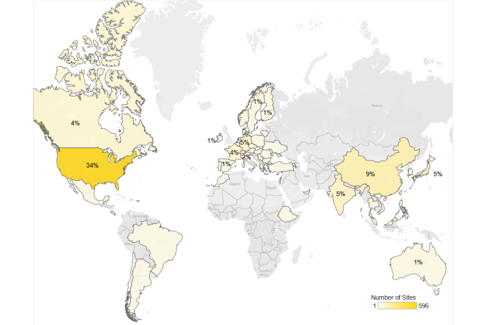
Source: Perspective Economics (n=2,195 sites)
Findings from consultations highlight the US as the dominant trade partner (home to customers and capital), followed by Europe (especially Germany, Ireland, the Netherlands and the Nordics), with Taiwan and China as critical Asia-Pacific links.
Stakeholders in different segments of the sector highlight that trade within the design-IP end of the value chain (US and APAC) looks geographically different from the manufacturing end, where Europe is more prominent given the presence of automotive OEMs.
Stakeholders suggest that supply chains are being reconfigured, with manufacturing being moved out of China, and to a lesser extent out of Taiwan, but that packaging remains a structural sector risk because it remains concentrated in those countries. Desk research supports these assertions. For example, a recent report on US Census Bureau trade data suggests that Mexico and Taiwan are overtaking China as sources of US advanced technology imports[footnote 27]. On packaging, a recent McKinsey article on barriers to scale in the US highlighted that lower cost Asian countries account for 75% of global supply of traditional assembly, packaging and test and that the concentration of advanced packaging is greater still[footnote 28]. Consultees also highlighted how Chinese restrictions in indium phosphide substrate exports are directly constraining UK activity. Some stakeholders suggested that the current geopolitical context offers a uniquely favourable opportunity for the UK to deepen relationships with similar-capability partners.
7.2 Semiconductor imports
HMRC trade data shows that since 2017 UK companies have spent an average of £2.9bn on imports of semiconductor goods each year (up from an average of £2.8bn in the baseline report). Having seen a marked increase between 2021 and 2022 (driven by increases in the unit cost of various types of integrated circuits), semiconductor import costs have remained relatively constant since 2023. A list of the harmonised system (HS) commodity codes used in this analysis is available in the appendices.
Figure 7.2 – Semiconductor imports
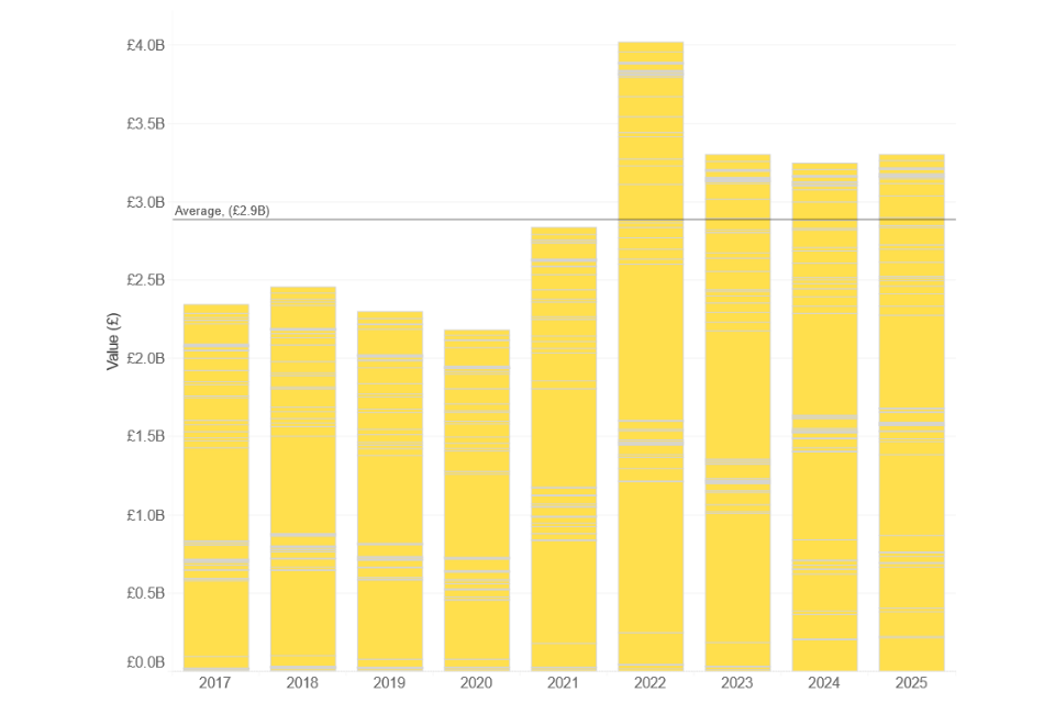
Source: HMRC UK Trade Info, Perspective Economics
79% of survey respondents indicated that they import products or services to enable their semiconductor business activity (n=44, baseline 75%, n=45). 70% of those respondents indicated that it would be beneficial to increase the share of semiconductor inputs procured from UK companies (n=31), but that those inputs are either not currently produced in the UK (cited by 81%, n=25) or that the cost of UK produced alternatives was prohibitive (cited by 71%, n=22). 55% of respondents who would like to diversify towards UK supply chains were not aware of UK alternatives (n=17). These patterns mirror those identified in the baseline study.
Table 7.1 – Barriers to UK supply chain diversification
| Response | Count | % of respondents |
|---|---|---|
| Availability of UK alternatives | 25 | 80.6% |
| Cost of UK alternatives | 22 | 71.0% |
| Availability of UK alternatives at suitable scale | 16 | 51.6% |
| Awareness of UK alternatives | 15 | 48.4% |
| Quality / consistency of UK alternatives | 14 | 45.2% |
| Other | 3 | 9.7% |
Source: Perspective Economics (n=31, respondents could select multiple options)
7.3 Semiconductor exports
70% of survey respondents indicated that they currently export semiconductor products or services (n=38). 50% of these respondents suggested that exports account for more than 75% of their total UK sales (n=18, baseline 60%). When asked which countries were most important for exports, 78% of respondents included both Europe and the US (n=28), with Europe ranked as a top priority market slightly more often than the US (17 respondents ranked Europe as their number one export market, compared to 14 who ranked the US as their top export market). A second tier of countries were cited by between 30% and 50% respondents, including China, India, Taiwan, Japan and ‘Rest of the World’.
HMRC trade data shows that semiconductor exports have grown by 23% since 2023 (£625k, Figure 7.3). This export growth has been driven by increases in exports of measurement and testing equipment and tools, which is a continuation of the trend seen in the baseline study.
Figure 7.3 – Semiconductor exports
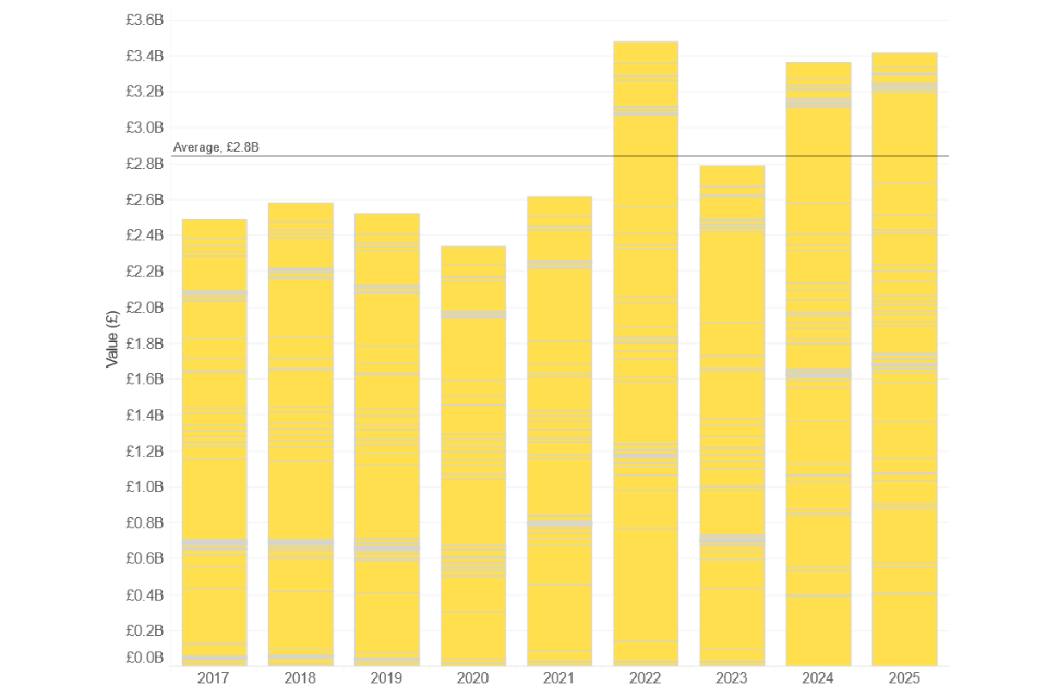
Source: HMRC UK Trade Info, Perspective Economics
7.4 Balance of trade
Increase value of semiconductor exports since 2023 means that the value of semiconductor related exports is now higher than the cost of semiconductor imports.
Figure 7.4 – Semiconductor trade balance
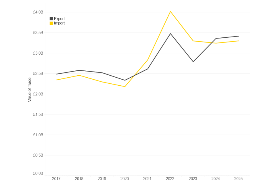
Source: HMRC UK Trade Info, Perspective Economics
Appendix 1: Research methodology
Purpose of this appendix
This appendix summarises how the Semiconductor Sectoral Analysis 2025 was produced. It sets out the approach used to identify UK firms with semiconductor activity, the data sources used, the checks applied, and the limitations that readers should consider when interpreting the findings. It is intended to be read alongside the main report.
The analysis builds upon the previous UK Semiconductor Sectoral Analysis published September 2024. The research provides an assessment of the number of businesses in the UK supplying semiconductor related products or services, the estimated contribution to the UK economy in terms of Gross Value Added (GVA), the estimated number of people employed in semiconductor roles, and an overview of the products and services offered by these firms.
How to read the estimates
Semiconductor activity in the UK is not captured by a Standard Industrial Classification (SIC) code. The study therefore adopts an experimental approach to identifying and measuring the economic contribution of semiconductor activity. All estimates within the study are experimental in nature and do not constitute official statistics.
They reflect a best estimate of the size and scale of semiconductor activity in the UK, derived from multiple official, commercial, and web-based sources, and are best used to indicate the broad size, scale, and composition of the sector, and to compare relative contributions across sub-sectors, regions, and firm sizes, rather than as precise values, particularly at the level of individual firms.
Research Scope
Consistent with previous studies, the analysis explores firms that:
- have a clear presence within the UK market, through a UK-registered business that reports to Companies House on an annual basis
- demonstrate an active provision of commercial activity related to semiconductors (e.g. via website / social media content)
- provide semiconductor products or services to the market (i.e. sell or enable the selling of semiconductor products or services to other customers)
- appear to be active at the time of writing (i.e. are not dissolved or in the process of dissolution)
- are not charities, universities, networks, or individual (non-registered) contractors – all excluded for analysis purposes
The study covers UK-registered businesses, including internationally headquartered firms with an evidenced UK trading presence. All estimates relate to UK activity only (i.e. reported or estimated UK revenue, employment, and GVA).
Companies are classified as ‘dedicated’ companies (typically smaller, specialised semiconductor companies whose business is built primarily around semiconductor products or services), or ‘diversified’ companies (typically larger companies with a broader offer, of which semiconductor-related products or services form a part).
Research limitations
This study is our best estimate of the size, scale, activity, and scope of the UK’s semiconductor sector. The boundaries of what constitutes the semiconductor ‘sector’ are contested and should be subject to a plurality of views and feedback, rather than definitively coded or classified. The following limitations should therefore be considered when interpreting the findings:
- Definitional subjectivity: there is no single agreed definition or classification for mapping the semiconductor sector. Definitional scoping and the use of web data are therefore required to identify relevant companies, and inclusion decisions reflect a best estimate by the research team using agreed parameters rather than a definitive classification.
- Fast-moving study boundaries: since the initial sectoral analysis in 2024, the tools and techniques used to identify, qualify and classify companies have improved significantly. Year-on-year changes may therefore reflect both genuine market change and methodological improvement, and comparisons over time should be interpreted with this in mind.
- Use of estimation techniques: where values are not available in full (e.g. via filed accounts), estimation techniques are applied on a per-employee basis, with ‘conservative’ low-end estimates applied for unknown values. Semiconductor-related activity among diversified firms is reported based on survey results.
- Quality and accuracy of self-reported data: financial and operational metrics for early-stage firms may be limited or unavailable via reported company data (e.g. unaudited or limited accounts). The analysis also requires matching of fields such as company name, registered number, and website across multiple datasets; several manual and automated steps are taken to minimise the risk of mismatch.
- Interpretation of text and language data: the identification of products, services and capabilities relies on descriptive web content and may overstate or understate the extent of a firm’s actual semiconductor activity or capabilities (e.g. due to the language used within branding and marketing content). Full web data may not also be available for some firms where web review is explicitly prevented. This is mitigated by use of wider sources, web search, and manual review.
- Survey and interview engagement: survey and interview findings rely upon voluntary engagement from firms and stakeholders. The sample is reviewed and prioritised to be reflective of the sector; however, responses may not fully represent the wider population of semiconductor firms.
- Point-in-time assessment: the analysis represents a point-in-time assessment of a dynamic market, with final checks undertaken in May 2026. Firms registered or materially changed after this point are not reflected within the study. Users should consider these limitations when interpreting findings and making strategic or policy decisions based on this research.
Research method
The study was produced in seven stages, summarised below.
Stage 1: Desk research and data discovery
The research team commenced with a desk-based review of semiconductor-related literature, news articles, company posts, and investment announcements (covering January 2025 to March 2026), to identify new programmes, progress, and key announcements across the UK semiconductor ecosystem, and areas for further focus. This informed: an updated list of semiconductor-related key terms to support identification (noting that keywords are only used to support potential longlisting, due to the risk of false positives or omissions); identification of web and wider sources for review; and a review of the 2024 baseline dataset to identify firms remaining active and in scope.
Stage 2: Initial longlisting
The identification stage aims to capture as many potentially relevant firms as possible within an initial ‘longlist’. This is deliberately broad: semiconductor activity spans multiple sectors including those involved in directly designing, manufacturing and / or packaging semiconductors, and those involved in providing the inputs required to enable direct semiconductor activity. The longlist drew upon a wide range of sources, including:
- the previous baseline (2024) dataset (with dissolved firms, and firms no longer in scope, removed);
- web data review, using weighted keyword matching and similarity searches across an internal dataset of UK-registered firms mapped to company websites;
- a review of newly active Companies House registrations within potentially relevant Standard Industrial Classification (SIC) codes;
- commercial and official sources, including Beauhurst (investment), FDI Markets (inward investment), HMRC Trade Info (trade in semiconductor-related commodities), Lightcast and anonymised web profiles (semiconductor-related employment), UKRI Gateway to Research (publicly funded semiconductor research), and Tussell (semiconductor-related public procurement); and
- a review of publicly announced accelerators, incubators, and early-stage growth initiatives.
All identified firms were collated into a single dataset, cleaned and deduplicated, assigned a unique ID, and enriched with known Companies House IDs and websites. This produced an initial longlist of potentially relevant firms for further review.
Stage 3: Taxonomy refinement
In December 2025, Perspective Economics held a taxonomy workshop with DSIT and expert advisors to test the study scope, definitions and categorisation (taxonomy). The updated taxonomy introduced fields to be captured, a lower level of granularity in supply chain mapping, and an expanded list of sectors and application areas commensurate with other international frameworks. The taxonomy is summarised below:
Stage 4: Final longlisting and enrichment
The longlist was subject to several quality checks including verifying web presence (all companies required an evidenced web presence for inclusion), verifying and validating the registered entity (reviewing websites and accounts to match each firm to the correct registered entity), deduplication, and removal of dormant or inactive entities. Following this, the refined longlist was subject to enrichment and review, including:
- enrichment against official and internal data sources (e.g. the Companies House API);
- a structured crawl of web data for each firm, reviewing the most relevant descriptive and trading content to identify descriptions, products, services, and use cases;
- an assessment of each firm’s relevance to the study using large language models (LLMs), tested via manual review against a sample of dedicated and diversified companies prior to application across the full dataset; and
- manual review across multiple quality metrics, with ‘edge’ cases resolved by expert review requiring clear evidence of creating or implementing semiconductor products or services.
Where websites prohibited the use of agentic review, this was respected, and the research team drew upon wider data (e.g. known descriptions, publicly filed accounts, and enhanced web searches). All firms carry evidence fields recording the content and source underpinning their inclusion. Final manual refinement removed non-commercial entities (e.g. university centres, membership bodies, charities, public bodies), companies with limited evidence of semiconductor activity, and companies without an evidenced UK trading presence.
Stage 5: Survey and qualitative engagement
Study briefings were undertaken with strategic stakeholders across UK regions in late 2025 to raise awareness and elicit expectations regarding the research. TechWorks conducted an online survey of 94 semiconductor firms in early 2026, administered via direct e-mail and an open weblink. The survey explored firm-level performance and industry perceptions, including extent of semiconductor business activity, business demographics (turnover, employment), semiconductor-related capabilities, products and use cases, perceptions regarding future growth, enablers and barriers, and expectations on international trade. The study team also conducted 38 in-depth interviews with strategic stakeholders across industry, academia, government policy and investment, with findings analysed thematically. An expert advisory panel was convened to test emerging findings and provide challenge regarding regional coverage and interpretation.
Stage 6: Final identification and shortlist
In April and May 2026, the research team revisited the dataset to undertake final additions and checks: review of survey responses against known values; identification of newly registered firms, and final cleaning and verification checks regarding registered entities, websites, and firms in scope. In total, 703 unique active firms were shortlisted for final analysis and inclusion in the study.
Stage 7: Sectoral modelling
Firms often sit across sectors and ecosystems. Further, some of the UK’s largest semiconductor related employers may hire hundreds of staff in their semiconductor teams but have thousands of employees across other functions. Extensive data cleaning, enrichment, and modelling is therefore required to develop semiconductor-related estimates of activity:
- Revenue and GVA estimation: known revenue and GVA values (from filed annual accounts of dedicated semiconductor companies) are used to estimate average and median revenue and GVA per employee, with quality review removing anomalies. These estimated values are banded by firm size and applied to estimated employment where values are unknown, with conservative low-end estimates used for unknown values. Known values are retained at the firm level. Estimates are reviewed against survey responses where appropriate (e.g. to account for pre-revenue firms). Null values are applied for early-stage firms with no or limited accounts data including employment.
- External investment: analysis of external investment matched company registration numbers to the Beauhurst platform for dedicated firms only. The research team only considers ‘dedicated’ activity to prevent over-estimation of semiconductor-related equity and VC investment. *Location data: all registered UK addresses and trading locations (UK offices identified via company websites) were reviewed, with markers for presence in each of the 12 UK regions and for country of origin (UK headquartered or internationally headquartered with a UK presence).
Quality Assurance
Quality assurance was applied at each stage of the research pipeline, combining automated checks with manual review throughout. In summary:
- Staged, evidence-based decisions: identification, deduplication, verification, classification, and enrichment were undertaken as distinct stages, so judgements are made using only the evidence relevant to that task. Rule-based checks and official data sources were used first, with large language models (LLMs) applied to ambiguous cases.
- Use of analytical tools, subject to human review: market-leading LLMs (typically Anthropic Claude models) were used to support the review, verification, and classification of firms at scale. Models were benchmarked and piloted before use, with manual validation and review gates prior to any full run.
- Conservative treatment of uncertainty: where evidence was limited, models were instructed to lean towards exclusion or omission. No firm was removed from the dataset without an evidenced rationale.
- Review with DSIT and expert stakeholders: the study scope, taxonomy, and emerging findings were reviewed with DSIT throughout, with an expert advisory panel providing further challenge and feedback.
Data sources
The data sources used to underpin the sectoral analysis, and their role within the study, are set out below:
| Source | Description | Role within the study |
|---|---|---|
| Web data (Perspective Economics) | Web content collated by Perspective Economics across company websites and wider web sources. | Identification of firms; classification against the agreed taxonomy; evidence base for products, services, and trading locations. |
| Bureau van Dijk FAME (and Companies House) | Collates Companies House data and financial statements from all registered businesses within the UK. | Verification of registered entities; company accounts data for employment, revenue and GVA analysis. |
| Beauhurst | Investment analysis platform enabling users to discover, track and understand the UK’s high-growth companies. | External investment raised (dedicated firms only); accelerator participation; supporting company information. |
| Lightcast | Labour market intelligence platform tracking job postings and anonymised employment profiles globally. | Identification of semiconductor-related skills and employment in firms. |
| FDI Markets | Identifies announced inward investment projects into the UK. | Identification of semiconductor-related inward investment and new market entrants within longlisting. |
| HMRC Trade Info | Publicly available data identifying UK companies importing or exporting against relevant trade and commodity codes. | Supporting signal of trading activity within the longlisting process. Analysis of semiconductor-related trade. |
| UKRI Gateway to Research | Publicly available data on companies in receipt of research and innovation funding. | Identification of firms engaged in publicly funded semiconductor research within longlisting. |
| Survey of semiconductor firms | Online survey of 94 self-reported semiconductor companies. | Firm-level performance and perceptions; calibration of modelled estimates. |
| Depth interviews | Semi-structured interviews with 38 stakeholders spanning industry, academia, government policy and investment. | Qualitative insight into growth drivers, enablers, and barriers. |
Appendix 2 – Long-form regional profiles
East of England
Technological focus
Cambridge’s semiconductor capability spans five complementary strands. The Semiconductor Physics Group (Cavendish Laboratory) leads on low-dimensional quantum systems, using GaAs/AlGaAs heterostructures and in-house MBE to study quantum devices, graphene, and spin-charge separation, with figures including Profs Ford, Hirst, Phillips, Smith and Sir Michael Pepper. The Cambridge Centre for Gallium Nitride (Materials Science) covers the full GaN chain - MOCVD growth, porous nitrides (commercialised via Porotech), GaN-on-Diamond for thermal management, and cubic-phase LEDs – anchoring the UK Nitrides Consortium. Next-generation materials research covers hafnium-oxide memristors for energy-efficient AI hardware, 2D semiconductors, halide perovskites, metal-organic frameworks, and chiral organic semiconductors. Cambridge’s 2D materials activity, anchored by the Cambridge Graphene Centre and the 2D Materials and Devices Group in Materials Science, is generating notable spinout activity — including CamGraPhIC (graphene photonic transceivers for AI interconnects, recently backed by a €211m Italian government/EU-approved package) and Molyon (MoS₂-based lithium–sulfur batteries, $4.6m seed). CASCADE, founded by a £3.5m Arm donation in 2024, trains 15 PhDs in architecture and design, complementing Cambridge’s CHERI capability architecture. Terahertz and photonics work delivers QCLs for 6G, imaging and sensing, with Cambridge participating in PIXEurope.
Cambridge is a globally leading semiconductor research and design ecosystem, with exceptional depth across fundamental quantum semiconductor physics, world-leading GaN and wide-bandgap materials capability, novel material platforms for energy-efficient AI computing, and globally significant chip architecture expertise through Arm and the CHERI/Morello Programme. Semiconductor activity deeply embedded across EDA, chip architecture, embedded systems, wireless, photonics and AI-specific processors.
The Cambridge semiconductor cluster is anchored by the University of Cambridge, through the Cavendish Laboratory’s Semiconductor Physics Group, the Department of Materials Science and Metallurgy, the Cambridge Centre for Gallium Nitride, and the new CASCADE Computer Architecture and Semiconductor Design Centre in the Department of Computer Science and Technology.
Application strengths
Cambridge’s semiconductor-relevant capability maps onto an exceptionally broad applications landscape, including AI and energy-efficient computing, quantum technologies, display and lighting applications, power electronics for electric transport and renewable energy, telecommunications and next-generation wireless applications, clean energy and sustainability, healthcare and life sciences, defence, security and secure communications, and Space applications.
Business base
Global processor design leader Arm has its headquarters in Cambridge and maintains close connections to the University of Cambridge, including via recent commitments to fund 15 PhD students over five years at the new CASCADE centre.
The regional business base has deep expertise in semiconductor design and intellectual property, including global-scale IP and fabless anchors through growth-stage spin-outs rooted in the University of Cambridge’s Materials Science and Metallurgy, Gallium Nitride and condensed matter programmes.
In addition to Arm, the East of England is home to design centres of several of the world’s largest fabless and integrated device manufacturers, including Qualcomm at Cambridge Business Park, Imagination Technologies at Kings Langley, MediaTek in Cambourne, and AMD and Synaptics at Cambridge Science Park.
Alongside these multinational anchors Cambridge is home to home-grown pure-play firms that are commercial translations of cluster research. Pragmatic Semiconductor in the north Cambridge cluster operates an IDM and foundry for flexible and ultra-low-cost thin-film integrated circuits. Paragraf, in St Ives, is a dedicated materials and device developer commercialising graphene-based semiconductor products, drawing directly on Cambridge’s condensed matter and materials research. CML Microcircuits in Maldon is a long-established pure-play fabless designer of wireless and wireline semiconductor ICs, Cambridge GaN Devices is a direct University of Cambridge spin-out focussed on commercialising integrated GaN power ICs for electrification markets, and Micross, which provides specialist back-end, packaging and assembly test services.
London
London hosts the institutional and strategic centre of gravity for the UK semiconductor sector, distinguished by its research universities, national coordination bodies, startup programmes, proximity to government, capital markets and major technology companies. The scale of adjacent co-ordination and advocacy activity in London is substantial. UKSC is backed by at least £19 million in government funding; the ChipStart UK programme’s first two cohorts (drawn from across the UK) collectively attracted approaching £30 million in venture capital and angel funding; and the Knowledge Quarter ‘innovation district’ at King’s Cross places UCL in close proximity to Google, DeepMind, Meta, ARIA and other organisations that depend on semiconductor technology as foundational to their products and services. London’s role as convening point for UK semiconductor policy, investment and coordination is reinforced by the geographic distribution of the UKSC team across the UK to support regional clusters.
Technological focus
London’s semiconductor research concentrates across four complementary strands. Interdisciplinary materials and device research at UCL’s Department of Electronic and Electrical Engineering, spans atomic-scale materials through to systems integration. UCL’s principal domains are photonics, quantum technologies, neuromorphic systems and two-dimensional materials. Of particular strategic significance, UCL leads UK efforts in neuromorphic computing and hosts an Innovation and Knowledge Centre (IKC) dedicated to its commercialisation. Supporting infrastructure includes the London Centre for Nanotechnology and the National Epitaxy Facility. The Optical and Semiconductor Devices Group at Imperial College London, founded in 1980, with microelectromechanical systems (MEMS) at its core alongside microoptical devices, organic semiconductors, energy harvesting, terahertz optics and single-atom silicon quantum electronics.
Beyond its research expertise, London provides the focal point for national sector coordination delivered by the UK Semiconductor Centre at the Institute of Physics, and an internationally prominent startup incubation initiative via Silicon Catalyst which delivers the ChipStart Pre-Seed Incubator and Two-Year Accelerator, with access to TSMC prototyping and more than 350 industry advisors.
Application strengths
UCL’s neuromorphic work and leadership of the neuromorphic IKC sits at the heart of a computing efficiency research and innovation focus, as does Imperial’s work on exceeding the speed barriers of silicon microelectronics. BlueShift Memory addresses related memory architecture challenges. Quantum technologies are represented through UCL’s quantum semiconductor expertise and Imperial’s single atom silicon quantum electronics research. Healthcare and life sciences applications feature prominently. UCL’s radar-based heartbeat monitoring project enables contactless health monitoring through semiconductor sensing and London-based ChipStart portfolio company MintNeuro is developing high-quality implantable medical devices for neural stimulation of the brain. Imperial’s biomedical applications strand extends to implantable sensors, diagnostic devices and therapeutic systems. Communications applications span UCL’s work on extremely wideband optical fibre communication systems, transforming networks through intelligent optical infrastructure, and 6G spectrum innovation in partnership with India; and Imperial’s terahertz optics and RF metamaterials for next-generation wireless and security imaging.
Business base
London’s semiconductor cluster is weighted towards design, IP and fabless activity, augmented by a relatively new cohort of research-led spin-outs. NVIDIA’s London operation is one of the most significant semiconductor-related employers in the capital, covering fabless chip design, EDA and IP activity. Lumentum, the photonic integrated circuit and optical networking IDM, maintains a meaningful London presence. Allegro Microsystems maintains a dedicated fabless chip vendor operation, while Semtech’s London site supports research, development and platform IP activity. Nanoco develops pure-play quantum dot and nanomaterial semiconductor products. Below these anchors sits a research-led cohort including DNA Electronics (DNAe), spun out of Imperial College (fabless chip vendor developing semiconductor-based genomic diagnostics) ESWIN (commercialising RISC-V and display driver semiconductor IP) Aion Silicon (ASIC design services) and Flexciton (pure-play EDA and manufacturing software).
North East
North East England is a business-led advanced electronics cluster with a focus on compound semiconductor industrial capability, next-generation material specialisms (diamond, flexible, organic), and adjacency to major industrial transformations in transport electrification and offshore wind. The cluster is organised around the North East Advanced Material Electronics (NEAME) cluster body and grounded in a long industrial heritage.
NEAME’s semiconductor focus is explicitly around technologies that go beyond conventional silicon, including compound semiconductors, two-dimensional materials, polymer and organic materials, and hybrid approaches. NEAME member companies span the full value chain, from raw electronic materials manufacture through microchip-scale device development, fabless design, and integration of advanced components into finished products. The region is involved in national semiconductor infrastructure through the Compound Semiconductor Applications Catapult’s NETPark site, and Newcastle University is part of the recently formed Centre for Heterogeneous Integrated MicroElectronic and Semiconductor Systems (CHIMES2) Innovation and Knowledge Centre (IKC).
Technological focus
Newcastle’s IKC research focuses on building next-generation integrated circuits that combine novel architectures with new generations of machine learning algorithms, such as Tsetlin machines, that are intrinsically built for low-complexity and scalability. By enabling modular and adaptable designs, researchers at Newcastle aim to help create a foundation for more future-proof and energy-efficient intelligent systems across a wide range of applications. Outside the university, the North East semiconductor cluster spans five complementary strands, including compound semiconductor RF and millimetre-wave components (e.g., Filtronic and Viper RF), compound semiconductor and MEMS manufacturing (e.g., INEX Microtechnology and Coherent materials engineering expertise), photonics and optoelectronics for space and aerospace (e.g., Axenic and Isocom) and flexible, organic and radiation detection electronics (e.g., Pragmatic Semiconductor, SmartKem and Kromek).
Application strengths
North East England’s semiconductor-relevant capability maps onto a diverse applications landscape including telecommunications and future networks, Space and satellite applications, defence, security and radiation detection, healthcare, flexible electronics, IoT, packaging and consumer applications including disposable sensors, smart packaging, wearables and connected devices, net zero, energy transition and power electronics applications, bridging the semiconductor cluster with the region’s wider industrial transformation, and an emerging focus on AI infrastructure and data centre applications.
Business base
The combination of established RF and mmWave industrial capability (Filtronic, Viper RF), optoelectronics for space (Axenic, Isocom), compound semiconductor and MEMS manufacturing (INEX, Coherent), frontier material platforms (Pragmatic Semiconductor, FlexIC, SmartKem organic, Kromek CZT detection), and proximity to substantial EV and offshore wind investment provides a commercial platform for regional semiconductor activity.
Coherent’s Newcastle operation is focused on materials development, fabrication consumables and equipment for the compound-semiconductor and photonic markets. With manufacturing facilities in Durham and production operations in Sedgefield, Pragmatic Semiconductor designs and manufactures flexible integrated circuits (FlexICs) that enable edge and item-level intelligence at scale and speed. Filtronic at Sedgefield is a dedicated fabless chip vendor, design services and back-end manufacturing firm focused on millimetre-wave and radio-frequency semiconductor products. Isocom in Peterlee is an IDM producing pure-play optoelectronic devices, and Tosoh Quartz in Stanley supplies dedicated semiconductor fabrication materials, specifically ultra-pure fused quartz wafers and components for fab processes. aXenic in Sedgefield, a CPI- and NETPark-linked spin-out, is a dedicated fabless chip vendor developing indium phosphide photonic devices for high-speed optical networks. Mignon Technologies in Newcastle is an early-stage pure-play fabless chip vendor. Nascent Semiconductor in Durham operates as a dedicated University-linked fabless and design services firm and EpiValence in Redcar provides dedicated fabrication materials and precursors for compound semiconductor epitaxy.
Northern Ireland
Northern Ireland is emerging as a notable semiconductor and photonics region, distinguished by a well-funded photonics cluster, a nationally influential hardware security research base, and a unique position within the cross-border Ireland / Northern Ireland funding landscape. Regional capability is anchored by Seagate Technology – global leader in mass-capacity data storage and lead partner within the £42m Smart Nano NI consortium[footnote 29] – with research and innovation activity supported by Queen’s University Belfast and Ulster University (both Smart Nano consortium members), and related research and innovation activity via the Queen’s University Advanced Micro-Engineering Centre (QAMEC)[footnote 30] centre of excellence for employing silicon MEMS microsystems technology in current and emerging sensor applications, and Ulster University’s involvement in the Cambridge-led Advanced Nanotube Application and Manufacturing Initiative (ANAM)[footnote 31] where carbon nanotubes show promise for future semiconductor applications. In addition to Seagate Technology, the local industrial base includes specialist photonics and sensor firms, and a maturing cluster structure operating under the Northern Ireland Photonics Innovation Cluster (NIPIC). In the North West cross-border initiatives such as the Semiconductor Photonics Education and Research (SPEAR) Centre are helping to position the region as a distinct semiconductor and photonics innovation hub, bringing together expertise from both the UK and the Republic of Ireland.
Technological focus
Northern Ireland’s semiconductor strengths span three complementary strands including integrated photonics and nano-manufacturing through the Smart Nano NI consortium, hardware security and secure-by-design research through the Centre for Secure Information Technologies at Queen’s, novel materials via Ulster’s involvement in ANAM, and commercial photonics and nano-manufacturing capability, anchored by Seagate Technology’s regional operations.
Application strengths
Semiconductor and photonics capability maps onto a focused applications landscape, spanning healthcare and medical diagnostics, data storage, optical communications and telecommunications infrastructure, quantum technologies, hardware security and secure-by-design applications, and compound semiconductor applications fundamental to photonic device manufacture.
Business base
Global technology company Seagate operates a large-scale (20-acre) advanced manufacturing plant processing silicon wafers to produce hard disk drive memory components, and holds a critical position in the global heat-assisted magnetic recording head supply chain. ICEMOS Technology is a silicon foundry operating in silicon-on-insulator wafers, high-voltage MOSFETs and MEMS, and providing one of the few dedicated small-volume foundry services in the UK. Raptor Photonics in Larne is a dedicated fabless chip vendor and equipment manufacturer producing EMCCD and InGaAs low-light cameras and imaging sensors. Wolfspeed’s Belfast-registered entity extends the region’s compound-semiconductor and SiC dimension and provides a direct connection to global wide-bandgap device supply. Arralis in Belfast is a dedicated fabless chip and design services firm producing monolithic microwave integrated circuits in gallium arsenide and gallium nitride for defence, space and aerospace markets, Amphion Semiconductor in Belfast operates as a dedicated platform IP licensing firm specialising in video codec and DSP IP, and AntennaWare in Belfast’s Titanic Quarter is a QUB spin-out developing dedicated antenna-on-chip semiconductor designs. Silansys is a pure-play mixed-signal ASIC design firm in Belfast. Brolis Photonics Solutions, in Larne, develops gallium antimonide mid-infrared laser diodes and is a dedicated photonic-device IDM. Causeway Sensors, another QUB spin-out, produces plasmonic semiconductor sensor devices for biosensing and environmental applications.
North West
Manchester hosts a distinctive and internationally significant semiconductor-adjacent materials research ecosystem, centred on two-dimensional materials and advanced functional materials research.
Relevance to the semiconductor sector is concentrated upstream in the fundamental materials science, characterisation infrastructure and national coordination that underpin the UK’s ability to move beyond silicon. Regional capability is anchored by the University of Manchester through the National Graphene Institute (NGI), its sister facility the Graphene Engineering Innovation Centre (GEIC), and by the Henry Royce Institute, the UK’s national institute for advanced materials research and innovation. The Royce’s hub-and-spoke model connects Manchester as the headquartered hub with the Universities of Sheffield, Leeds, Liverpool, Cambridge, Oxford, and Imperial College London as spokes, creating a national network of expertise directly spanning most of the UK’s principal semiconductor-active regions. Manchester is also a CHIMES² IKC member.
Technological focus
Manchester’s semiconductor-relevant strengths span three complementary strands including two-dimensional materials research and fabrication, industrial translation through the GEIC (whose partners include BAE Systems, Honda, Haydale, Smart IR (infrared sensing), Levidian and the National Physical Laboratory). Printed electronics is a particular commercial focus, with graphene enabling flexible displays, wearable sensors, RFID tags and thin-film transistors, and national coordination through the Henry Royce Institute’s Atoms to Devices programme. Royce Technology Platforms span physical vapour deposition, thin film devices, doping, and ultra-high vacuum 2D materials assembly, distributed across Cambridge, Imperial, Leeds and Manchester.
Application strengths
Manchester’s 2D materials and advanced functional materials capability maps onto a broad applications landscape spanning post-silicon electronics, photonics and optoelectronics, quantum technologies, sensing, and flexible and printed electronics. Post-silicon electronics is the most distinctive and forward-looking application strength, thermal management applications draw on graphene’s thermal properties to address heat dissipation, photonics and optoelectronics applications draw on the unique optical and electronic properties of 2D materials across sensors, photodetectors, and light-emitting devices, and quantum computing and quantum technologies applications draw on the quantum mechanical properties of certain 2D materials as candidates for quantum computing components. Infrared sensing and thermal imaging are commercially visible through the Smart IR partnership, with applications ranging from medical diagnostics and environmental monitoring to defence and security systems. Flexible and printed electronics applications are central to the GEIC’s commercial positioning, spanning flexible displays, wearable sensors, RFID tags and thin-film transistors. Defence and aerospace electronics applications are anchored by the BAE Systems and GKN partnerships, covering radar systems and advanced sensing technologies with significant semiconductor content. Automotive applications span advanced driver assistance systems, EV battery technologies, and thermal management systems for power electronics, anchored by the Honda partnership. Memory and data storage applications are a specific commercial focus, and bioelectronics and healthcare sensing applications connect 2D materials research to diagnostics and treatment. Energy applications are cross-cutting, spanning solar cells, power electronics for renewable energy systems, and the sensors and control systems needed for complex energy networks.
Business Base
The regional industrial cluster is weighted towards multinational IDM and fabless activity concentrated in Stockport, Greater Manchester and Cheshire, with a supporting layer of materials, IP and early-stage spin-out activity. Nexperia at Stockport is the largest dedicated semiconductor employer in the region, operating as an IDM focused on discrete, logic and MOSFET semiconductors. Graphcore, also in Stockport, operates as a fabless chip vendor, provides EDA software and design services, and is one of the UKs most significant dedicated AI-accelerator semiconductor firms. Intel maintains a Manchester city-centre design and software operation, Texas Instruments operates an IDM-supporting site at Manchester Airport focused on power management and analogue semiconductor design and application engineering. Diodes, in Oldham, extends the Cheshire IDM footprint with dedicated discrete and analogue semiconductor manufacturing-support activity.
Beyond these core semiconductor firms, SmartKem in central Manchester is a dedicated materials and IP developer commercialising organic semiconductor thin-film transistors for flexible displays, Integrated Compound Semiconductors, in Cheadle, is a pure-play IDM focused on compound semiconductor devices, Quantum Science in Warrington produces dedicated semiconductor nanomaterials, Plus Opto in Wigan provides pure-play design and packaging services for photonic devices, sureCore in central Manchester is a dedicated IP and design firm specialising in low-power memory IP for the fabless design community, and Codeplay Software provides dedicated EDA and design services.
Scotland (Edinburgh)
Edinburgh is a research-and-fabrication centre with expertise in the integration of physical capability, emerging device science, and AI-hardware co-design. The Scottish Microelectronics Centre (SMC) provides an industrial-standard fabrication and characterisation platform rarely found outside commercial fabs, giving the region an unusual ability to prototype and validate processes at scales directly transferable to manufacturing.
The Centre for Electronics Frontiers delivers world-class work on the post-CMOS device paradigms; memristors, neuromorphic architectures, adiabatic computing, and heterogeneous integration, that are increasingly recognised as essential to a sustainable AI compute future. The APRIL AI Hub positions Edinburgh at the centre of a national network applying AI systematically to the electronics supply chain itself, from materials discovery through verification and testing. Complementary work on wafer-scale software frameworks, bioelectronics, flexible and printable electronics, energy harvesting, and radiation-resilient devices extends the portfolio across most of the high-value applications areas identified in UK strategic thinking. The combined effect is a regional capability that is both deeply vertically integrated — from cleanroom through device physics to systems and software — and aligned with the headline structural challenges facing modern electronics: energy efficiency, scaling beyond CMOS, and the productivity gap in research and design workflows.
Technological focus
Edinburgh’s semiconductor research concentrates across three complementary strands. In fabrication, characterisation and MEMS capability is delivered via the Scottish Microelectronics Centre’s (SMC’s) 250-square-metre cleanroom; providing lithography, dry etching, metallisation, wet processing and inspection on wafers up to 200mm, aligning with industrial substrate norms and supporting direct process transfer to commercial environments. SMC offers a comprehensive up to 200mm toolset, offering deep characterisation (XPS, Raman, REELS, AFM) and parametric testing via HP and Keithley analysers. End-to-end services from mask design through wafer fabrication to chip post-processing, alongside hosting space for small companies, make it a practical bridge between research and industrial readiness. Beyond-CMOS, neuromorphic and AI-hardware research at the Centre for Electronics Frontiers (CEF) maintains relationships with over one hundred global companies and pursues memristors, neuromorphic architectures dissolving the Von Neumann bottleneck, and silicon demonstrators including NeuroStripe, ACNN1-3, MELITA, Aggregator and ASOCA chips. Complementary themes span bioelectronics, flexible electronics and radiation-resilient devices. The AI for Productive Research & Innovation in eLectronics (APRIL) hub aspires to unite the electronics and AI communities for developing and bringing AI-based tools to market that will boost productivity across the entire electronics industry supply chain. The APRIL hub links 20 universities and 30+ industry partners across five innovation pillars.
Application strengths
The applications landscape served by Edinburgh’s semiconductor research spans both near-term commercial domains and frontier sectors. Sensing and measurement is a particular strength, reflected in SMC industrial partnerships including Pyreos (thin-film pyroelectric sensors), NuNano (AFM probes), and Silson (ultra-thin membranes). Future communications activity is driven by the Institute for Imaging, Data and Communications (IDCOM)[footnote 32] at the University of Edinburgh, involving a broad base of multi-disciplinary teams. Memsstar Technologies anchors the cluster’s engagement with deposition and etch equipment for semiconductor and MEMS manufacturing globally.
AI hardware applications dominate CEF’s and APRIL’s external reach, addressing sectors under acute pressure from the energy cost of conventional computing. Target application domains include healthcare (diagnostic tools, responsive medical devices, brain-computer interfaces), space exploration (smarter spacecraft and satellites requiring local AI inference under strict power budgets), automotive systems, robotics, security and defence. The bioelectronics work on neural interfaces and memristor-brain-silicon coupling has direct medical device relevance, and the radiation-resilient electronics theme serves space, healthcare and defence specifically.
Sustainability is a cross-cutting application theme, manifest in CEF’s work on recyclable and sustainable electronics, energy harvesting through organic semiconductors suitable for large-scale printing, and APRIL’s engagement with green algorithms and GREENER principles through its sustainability workshop series.
Business base
A cohort of dedicated semiconductor firms constitute the commercial heart of the east-of-Scotland cluster. Shin-Etsu at Livingston is a large silicon substrate operation and the principal wafer-supply node in the wider European electronics supply chain. Cirrus Logic maintains a substantial Edinburgh design centre focused on high-performance mixed-signal and audio fabless design. Semefab in Glenrothes is one of very few UK-owned silicon foundries, providing specialised analogue, MEMS and power process technology. Clas-SiC Wafer Fab, also in Fife, delivers dedicated silicon carbide wafer fabrication for third-party customers and is the only UK-based pure-play SiC foundry. Sivers Semiconductors adds a further wide-bandgap and optical fabless/IDM dimension.
The cluster is also home to several specialist pure-play firms including, for example, Dukosi (dedicated battery cell monitoring chip design), Alter Technology (dedicated semiconductor test, engineering and space-grade evaluation services), pureLiFi (LiFi modulator and receiver chipsets), Memsstar (MEMS etch and process equipment for fabrication tool markets) and Gas Sensing Solutions in Cumbernauld (non-dispersive infrared semiconductor gas sensors). Cirrus Logic draws on the University of Edinburgh’s strong analogue and digital design talent pipeline. Semefab and Clas-SiC operationalise the region’s only volume silicon and SiC foundry capacity within analogue, MEMS, power, and wide-bandgap sub-segments.
Scotland (Glasgow)
Glasgow hosts one of the UK’s most substantial and historically rooted concentrations of semiconductor and photonic technology capability. The regional capability is anchored by the University of Glasgow, the University of Strathclyde (via the Institute of Photonics and the co-located Fraunhofer Centre for Applied Photonics), and a wider industrial and innovation network coordinated through Photonics Scotland. The scale of this ecosystem is significant: the Scottish photonics sector, most of which is concentrated in and around Glasgow, generates over £1.2 billion in annual turnover, employs approximately 6,400 people in high-value roles, and exports 97 per cent of its output. Photonics Scotland serves a community of over 50 companies alongside a globally recognised academic base.
Cluster capabilities span a broad semiconductor and photonics ecosystem including device physics, advanced packaging and automation, photonic and laser technology, and applied research and development. The University of Glasgow’s advanced semiconductor packaging facility (ANALOGUE) offers automated packaging and characterisation capability, addressing one of the most strategically important emerging areas of semiconductor technology worldwide, with built-in provision for UK-wide remote access. The Institute of Photonics and Fraunhofer Centre for Applied Photonics (CAP) together constitute one of the UK’s most substantial concentrations of applied photonic and laser technology expertise, with particular depth in quantum, mid-infrared and GaN micro-LED domains.
Technological focus
Glasgow’s semiconductor research concentrates across four complementary strands. The ANALOGUE facility offers advanced semiconductor packaging and automated processing, including a fully automated platform spanning device-level work to complete application development with integrated workflow design and live analytics. Its orientation towards additive packaging aligns with the industry shift to chiplet integration, 3D stacking and heterogeneous integration, and remote access to UK researchers positions it as a resilience-building national resource. Silicon-compatible device physics, quantum-enabled sensing and mid-infrared photonics research is delivered by the Semiconductor Device Group, which leads the UK Hub for Quantum Enabled Precision Navigation and Timing and partners the Integrated Quantum Network Hub. Its portfolio spans MEMS gravimeters (now demonstrating Earth tides measurement), Germanium-on-Silicon Single-Photon Avalanche Diodes (Ge-on-Si SPADs) for LiDAR, chip-scale atomic spectrometers, silicon nanowires, mid-infrared waveguides and SiGe terahertz quantum cascade lasers, unified by a strategic emphasis on CMOS compatibility. GaN micro-LED technology at Strathclyde’s Institute of Photonics has focussed on the fabrication of micro-LEDs since 2002 and remain at the leading edge of research. Applied laser and photonic technology at Fraunhofer CAP, the UK’s first Fraunhofer centre, delivers solid-state, mid-infrared and semiconductor disk lasers, flagship QT Assemble, and STREAMLINE projects, partnered with the Fraunhofer Institute for Applied Solid State Physics (IAF).
Application strengths
Glasgow’s semiconductor-relevant capability maps onto an exceptionally broad applications landscape. Quantum technology is a key strength and cuts across all four research strands. Work on quantum-enabled position, navigation and timing via MEMS gravimeters and cold-atom systems, the Institute of Photonics’ QuantIC partnership, Fraunhofer CAP’s quantum sensing, imaging, communications and computing programmes, and Glasgow-originated spin-out Kelvin Quantum’s cryogenic electronics for quantum computing collectively give the region vertical depth in quantum. Healthcare and biomedical applications feature strongly through the Institute of Photonics’ neurophotonics work, the Mathieson bionic eye implant, GaN micro-LED optogenetics, breath analysis sensors, and the mid-infrared medical diagnostics applications of germanium-on-silicon waveguide work. Space and satellite applications are a major regional priority given that Scotland produces more small satellites than any other European country, and has an explicit ambition to provide a complete European solution for small satellite manufacture and launch. Photonics Scotland’s dedicated Photonics for Space Special Interest Group (developed with the Higgs Centre for Innovation) supports member access to this market, with Simera Sense and Fraunhofer CAP’s space contract research representing active delivery. Defence and security applications draw on mid-infrared spectroscopic laser capability at Fraunhofer CAP, laser range-finding and target designation, line-of-sight communications, LiDAR, and directed infrared countermeasures. Communications applications include the Institute of Photonics’ role in the TITAN telecommunications hub (one of three UK national telecommunications hubs funded by UKRI), visible light communications and Li-Fi, high data rate optical communications. The Scottish photonics sector retains established strengths in lasers (e.g., Coherent in Glasgow, Skylark Lasers) and optical transceivers. Glasgow spin-out AIDE is applying AI to antenna, analogue and RF IC, and filter design, targeting productivity gains in component design workflows. Energy and sustainability applications span Fraunhofer CAP’s wind LiDAR for offshore turbine protection, the Institute of Photonics’ mask-free lithography enabling more sustainable small-volume semiconductor prototyping, the Semiconductor Device Group’s historical thermoelectric and photovoltaic work, and the broader sector’s Race to Zero commitment through Fraunhofer CAP and Photonics Scotland’s sustainability agenda. Glasgow spin-out RX Watt’s simultaneous wireless power and data transfer technology addresses battery-dependent sensing across industrial monitoring, smart infrastructure, healthcare and environmental sensing. Advanced imaging and sensing applications include Singular Photonics’ SPAD-based image sensors, Mapix Technologies’ LiDAR and 3D sensing solutions, and the broader mid-infrared sensing work across the ecosystem.
Business base
Future Technology Devices International (FTDI), headquartered in Glasgow, is the largest dedicated semiconductor employer in the Central Belt, providing a long-established portfolio of USB, serial and bridge ICs used in tens of millions of devices worldwide. Synaptec, also Glasgow-based, is a pure-play fibre-optic sensor and photonics integration firm developing dedicated semiconductor and photonic instrumentation for electricity grid monitoring. Ichor Systems in central Glasgow supplies semiconductor fabrication tools, gas delivery and fluid delivery subsystems to global semiconductor equipment manufacturers. Retronix Semiconductor in Bellshill delivers specialist wafer, component and equipment services to the semiconductor supply chain and is a rare example of a UK-based dedicated semiconductor services firm with genuine equipment and back-end capability. A cluster of dedicated spin-outs and scale-ups gives the Glasgow ecosystem its most distinctive character. Vector Photonics, a James Watt Nanofabrication Centre (JWNC) and University of Glasgow spin-out, develops dedicated photonic crystal surface-emitting lasers in gallium arsenide and indium phosphide. III-V Epi, operating out of the JWNC, delivers dedicated compound-semiconductor epitaxy and pilot foundry services and is a direct commercial expression of the JWNC’s research infrastructure. Neuranics, another Glasgow-Strathclyde spin-out, produces pure-play magnetic sensor semiconductor ICs for neural interfaces. Kelvin Quantum, a University of Glasgow quantum-hardware spin-out, sits in the dedicated fabless and design layer targeting quantum semiconductor devices. Semiwise, based in Glasgow’s west end, operates as a dedicated design and IP house specialising in advanced silicon device simulation and sub-7 nanometre IP. Antonine Technology and Probe Test Solutions, respectively provide dedicated IP/design services and pure-play semiconductor probe test capability to wafer producers.
South East (Southampton)
Southampton hosts one of the UK’s most strategically significant and infrastructure-rich semiconductor research centres, distinguished by world-leading silicon photonics capability, uniquely advanced fabrication infrastructure, and a pivotal position as joint or partner institution in multiple national programmes. Regional capability is anchored by the University of Southampton – particularly the Optoelectronics Research Centre, the Electronics and Computer Science department, the Zepler Institute’s adjacent research groups, and the Southampton Nanofabrication Centre – supported by the CORNERSTONE silicon photonics foundry operated jointly with the University of Glasgow and the Science and Technology Facilities Council (STFC). Southampton’s current role spans CHIMES-IKC joint leadership with Sheffield, EXPRESS programme joint leadership with Warwick, NEF pump-priming partnership, QuantIC consortium membership, and partnership in the Fraunhofer CAP-led QT Assemble project. The Southampton Nanofabrication Centre’s 200mm wafer industrial-standard fabrication infrastructure – with the first electron beam lithography system of its kind outside Japan – is a distinctive national asset.
Technological focus
Southampton’s semiconductor strengths span four complementary strands including silicon photonics foundry and rapid prototyping through CORNERSTONE, advanced nanofabrication infrastructure at the Southampton Nanofabrication Centre, nonlinear semiconductor photonics, developing alternative material platforms for wavelength conversion, frequency combs and entangled photon pair generation, and systems-level leadership through the Optoelectronics Research Centre bridging fundamental research and foundry prototyping.
Application strengths
Southampton’s semiconductor and photonics capability maps onto a broad applications landscape spanning telecommunications and high-speed data communications, sensing applications including environmental sensing, biosensing, and chemical detection, LiDAR (driven primarily by automotive industry demand for three-dimensional sensing for autonomous vehicles), quantum technologies, AI hardware with photonic integrated circuits for AI inference and training offering potential bandwidth and energy advantages, health technology and medical diagnostics applications, defence applications, MEMS and NEMS device applications spanning inertial sensing, pressure measurement, microfluidics, RF filtering, and energy harvesting, photovoltaics applications, heterogeneous integration and advanced packaging applications.
Business base
Synopsys in Bracknell operates as the UK centre for the world’s largest dedicated EDA software and platform IP firm. Cadence Design Systems, also in Bracknell, hosts a second major global EDA centre. Broadcom in Reading is a dedicated fabless chip vendor and IDM with a substantial UK design and applications engineering footprint. Renesas Electronics in Bourne End and NXP Semiconductors in Romsey each run IDM, fabless, platform IP and design-services operations, giving the region deep exposure to the global automotive and industrial semiconductor supply chain. Micron Technology in Bracknell adds dedicated memory IDM and discrete memory device activity, STMicroelectronics in Marlow is a dedicated IDM with front-end fab and back-end manufacturing activity and Microchip Technology in Wokingham completes a multinational IDM cluster. A growing cohort of pure-play UK-headquartered firms complements the multinational base. EnSilica in Abingdon is a dedicated ASIC design-services and fabless chip vendor, MacDermid Alpha (formerly Compugraphics) in Woking supplies dedicated photomasks to the European semiconductor industry and represents a rare UK-based link in the lithographic supply chain.
South West (Bristol)
Bristol is emerging as a nationally significant centre for semiconductor research, anchored by the University of Bristol, with a breadth of activity spanning power electronics, RF and 6G communications, advanced materials characterisation, and quantum engineering. It is currently predominantly research-led, with emphasis on frontier ultra-wide-bandgap power semiconductors, internationally relevant RF and 6G research, and a commercially oriented advanced characterisation service. A key strength is upstream, in materials science, device design, RF and power electronics research, and the characterisation infrastructure needed to translate novel materials into deployable devices.
Combined with a dense industrial partner network reaching major international players (Bosch, Hitachi Energy, GE Vernova, Toshiba, Renesas, ST Microelectronics, onsemi, Siemens, Vishay) alongside UK specialists (Cambridge GaN Devices, Clas-SiC Wafer Fab, IQE, Element Six), Bristol is a prominent location for supporting transition from laboratory breakthrough to commercial deployment.
Technological focus
Bristol’s semiconductor research concentrates on three complementary strands, underpinned by substantial cross-cutting infrastructure.
The first strand is next-generation power semiconductors, pursued through REWIRE under Professor Martin Kuball. Bristol operates what was Europe’s first Agnitron Agilis 100 MOCVD reactor for β-gallium oxide epitaxy, a frontier ultra-wide-bandgap material with theoretical potential to outperform silicon carbide and gallium nitride in high-voltage power electronics. The university has demonstrated first-of-their-kind vertical Schottky diodes with breakdown voltages exceeding 4 kV, with the Ga₂O₃ programme currently at TRL 3 and focused on dielectric and etching improvements. Bristol also contributes to GaN device research and participates in a REWIRE workstream on Extreme Environment Electronics relevant to aerospace, defence and nuclear.
The second strand is RF and 6G communications, evidenced by a May 2025 Nature Electronics paper led by Kuball on GaN radio frequency amplifiers that delivers step-change switching speeds, output powers and reliability required for 6G. This work sits alongside the Smart Internet Lab, whose Director Professor Dimitra Simeonidou was appointed Chief Scientific Advisor to the European Commission in May 2025.
The third strand is advanced materials characterisation through the Centre for Imaging Facilities, offering commercially available FIB-SEM-TEM capability for device failure diagnosis. Supporting infrastructure includes the Centre for Nanoscience and Quantum Information and multiple CDTs.
Application strengths
Bristol’s semiconductor-relevant research maps onto several strategically important application domains. Electric transport and charging infrastructure is a primary focus of the REWIRE work, with all-electric trains, ships and heavy goods vehicles highlighted as target platforms alongside conventional EV powertrains. Wide-bandgap devices are identified as the enabling technology for the voltages and currents involved, which push silicon to its operational limits. Renewable energy and grid infrastructure is a second major application domain, including High Voltage Direct Current (HVDC) connections for offshore wind and intelligent power distribution to accommodate variable renewables and battery storage. Data centre power conversion is flagged specifically in the context of AI-driven demand growth, where efficiency gains from compound semiconductor power electronics translate directly into reduced energy consumption and carbon footprint. In the RF and communications domain, Bristol’s 6G work targets remote healthcare diagnostics, remote surgery, advanced driver assistance, fully autonomous vehicles, industrial automation, virtual classrooms, and haptic communication. Materials characterisation services at the University support a complementary set of application areas, including chip failure analysis, electronics quality assurance, consumer electronics and payments, medical devices, and potentially next-generation semiconductor architectures and quantum hardware. Defence, aerospace and nuclear feature through REWIRE’s Extreme Environment Electronics workstream, with partners including the UK Atomic Energy Authority. Electric aviation is represented through partnerships with Ampaire and Sora Aviation.
Business base
The regional business base is well-aligned with the wide bandgap, radio frequency, quantum and photonic research agendas anchored at Bristol, Warwick and Cambridge through REWIRE, the University of Bristol’s materials analysis and Gallium Nitride programmes, and the Cabot Institute’s net zero platform. In Plymouth, Plessey Semiconductors is an IDM with front-end fab capability, whose focus on Gallium Nitride microLED and power device technology sits squarely within the wide bandgap research mission of REWIRE. Equipment and tools manufacturer Infineon maintains a sizeable Bristol site combining IDM, foundry interface and design activity in the wider Stoke Gifford corridor, reinforcing the region’s proximity to commercial SiC and GaN power electronics alongside Warwick’s SiC CVD reactor and Cambridge’s GaN epitaxy. Effect Photonics in Torbay is a pure-play fabless designer of photonic integrated circuits for coherent optical transceivers, aligned with the Smart Internet Lab and the 5G-to-6G research agenda described earlier. XMOS in central Bristol is a dedicated fabless chip vendor producing xCORE processors for voice and audio edge AI, and Blu Wireless Technology, also Bristol-based, develops millimetre-wave RF semiconductor platforms for fixed wireless access and transport connectivity; a direct commercial translation of GaN RF amplifier research at the University.
In addition to these larger businesses, a second tier of dedicated semiconductor firms gives the region a distinctive profile. Swindon Silicon Systems, at Royal Wootton Bassett, provides dedicated mixed-signal ASIC design services, Codasip, in the Temple Quarter, is a dedicated processor IP and EDA firm active in RISC-V, linking the region to the fabric of CPU intellectual property. Lew Techniques in Taunton delivers specialist back-end and packaging consumables used by semiconductor assembly and test operations, IES Semiconductor Parts, in Avonmouth, sits at the intersection of equipment manufacture and fabrication materials, supplying front-end tools, KETS Quantum Security, a University of Bristol spin-out, develops chip-scale quantum key distribution devices drawing directly on the Centre for Nanoscience and Quantum Information and the Quantum Engineering CDT.
Wales (South Wales)
South Wales hosts one of the UK’s most clearly defined and institutionally mature semiconductor clusters, distinguished internationally as the world’s first compound semiconductor cluster.
The ecosystem grew from a collective vision set out in 2015 and has since become recognised as a strategic national asset, with deep alignment between universities, industry, the public sector and global investors. The South Wales cluster has deep-specialism in compound semiconductor materials, devices and applications that complement silicon CMOS, and that are key to UK strategic priorities in net zero, sovereign 5G/6G telecoms, quantum, defence electronics and AI infrastructure. The cluster hosts a near end-to-end vertical supply chain, two major university-anchored research centres, a national Catapult, two dedicated CDTs (in compound semiconductor manufacturing at Cardiff and in semiconductor skills at Swansea)[footnote 29], and sustained multi-source public invest. In addition to its unique position as a compound semiconductor cluster, the region also has semiconductor process tool and metrology equipment manufacturing as an indigenous capability. This capability creates an integrated capability that spans research, innovation, pilot lines, specialist equipment and high-value manufacturing across a 70-mile corridor from Chepstow to Swansea, and provides substantive local supply chain opportunities that support jobs both up and downstream.
Technological focus
The cluster’s defining specialism is compound semiconductors, including gallium nitride, silicon carbide, indium phosphide and emerging wide-bandgap and photonic materials. This specialism is reinforced by a near-complete vertical supply chain spanning epitaxial materials growth, wafer manufacturing, device fabrication, advanced packaging, module integration and systems, and process tool and metrology equipment manufacturing. Research and translation capacity is concentrated in three strongly complementary institutions. The Compound Semiconductor Applications Catapult in Newport provides national-level applications and commercialisation expertise including within power electronics, RF and microwave, photonics, and advanced packaging. The Compound Semiconductor Centre, established by IQE and Cardiff University, now operating as a collaborative centre for advanced epitaxy and semiconductor materials development. The Institute for Compound Semiconductors (ICS) at Cardiff University is a purpose-built research facility enabling device development and manufacturing scale-up. Swansea University’s Centre for Integrative Semiconductor Materials (CISM), based at the Bay Campus, opened a £29.9 million RPIF-funded facility in 2023 with partners including IQE, KLA and Vishay Newport. CISM works across advanced silicon, compound semiconductors (particularly wide-bandgap materials for power as a speciality) and emerging “soft” semiconductors (two-dimensional materials, organic semiconductors and perovskites), and houses the National Metal-Organic Chemical Vapour Deposition (MOCVD) Facility for chalcogenides and ultra-wide-bandgap oxides, ISO-qualified clean rooms, and backend packaging lines. CISM also hosts the UK’s National Pilot Line for SiC power component development (Driving the Electric Revolution) and is the only example in the UK of a translational pilot fab designed on industrial principles as a high up-time ballroom. Collectively over the past decade, more than £850 million has been invested in research, pilot fabrication, manufacturing, and innovation facilities across the region.
Application areas
Regional capability aligns with several strategically important UK markets, including AI infrastructure, quantum technologies, defence, communications and sensing, power electronics for electric vehicles, and net zero applications including charging infrastructure and grid applications. Major R&D programmes include:
- Strength in Places Fund – CSconnected: £43M programme embedding coordination, capability building and skills development (2021–2026).
- Future Compound Semiconductor Manufacturing Hub (EPSRC): multi-university collaboration led by Cardiff.
- Centre for Doctoral Training in Compound Semiconductors @ Cardiff and Centre for Doctoral Training in Semiconductor Industry Future Skills @ Swansea >120 PhDs trained for industry and academia.
- Driving the Electric Revolution (UKRI): supporting next-generation power electronics and sovereign supply chains for electrification.
- Place-Based Impact Accelerator Account (PBIAA): Cardiff and Swansea partnership accelerating regional innovation capacity.
Business base
South Wales is home to the commercial heart of the UK’s densest compound-semiconductor cluster. The cluster runs from substrate and epitaxy through front-end fab, photomask supply, pilot-scale devices, specialist equipment and materials chemistry, through to design-automation and pilot-scale photonic devices. IQE sits at the apex of the cluster, with it’s main plant in Newport (Imperial Park) and a secondary plant at St Melons, giving South Wales a global position in epitaxial wafer supply for compound-semiconductor devices across radio-frequency, photonic and power markets. IQE and Vishay are supported by substantial epitaxy capabilities within both Cardiff and Swansea universities, and Swanea is now running a commercial epitaxial foundry service for ultra-wide bandgap materials. IQE is the single largest dedicated compound-semiconductor epitaxy firm in the UK and one of the principal industrial anchors of CSconnected. Vishay Newport operates the 200-millimetre silicon and compound-semiconductor wafer fab at Duffryn giving South Wales volume front-end manufacturing capability, and KLA’s Newport operation designs and builds advanced etch, deposition and wafer-processing equipment for semiconductor manufacturers worldwide. Microchip Technology in Caldicott provides leading edge advanced semiconductor packaging services, focussing on miniaturized, high-reliability modules for aerospace, defence, medical and industrial sectors, and serving as a key hub for Microchip’s European operations. All of these core anchor firms (and others) have delivered major expansions, supporting manufacturing growth and specialised equipment capability.
In addition to the three South Wales anchor firms sits a substantial cohort of further specialist semiconductor businesses, including but not limited to Photronics (semiconductor photomask supplier and one of the few UK-based firms at that layer of the supply chain, serving both the compound-semiconductor cluster around it and the wider UK fabless community), and smaller, specialist firms that extend the cluster into design (Novomorphic, Thalia Design Automation), materials chemistry and innovation support (Irresistible Materials, Kubos Semiconductors), and pilot-scale photonics (Ffotoneg).. Space Forge is using space-derived crystal seeds to grow ultra-high quality semiconductor substrates on Earth for the next generation of power electronics, telecommunications and quantum technologies. Founded in 2018, the company now has a base facility in Rumney and are incubated in CISM for CVD reactor development.
West Midlands
Warwick hosts a focused and technically ambitious semiconductor research programme concentrated at the University of Warwick, with deep capability in group-IV semiconductor materials physics, a strong emphasis on silicon-compatible quantum and next-generation electronic materials, and a comprehensive shared nanofabrication infrastructure. Regional semiconductor capability is anchored by the Semiconductors Research Group within the Department of Physics, the Nano Fabrication Research Technology Platform and the EXPRESS programme – a £10.4 million five-year EPSRC-funded initiative jointly led with the University of Southampton. Institutional depth includes the EPSRC Centre for Doctoral Training in Diamond Science and Technology, the Warwick Manufacturing Group, the Warwick Innovation District, and active engagement with the UK Microsystems Network (an EPSRC-funded initiative launched in March 2025 with thirty-two partner organisations). The original Science City cleanroom partnership with the University of Birmingham reflects the collaborative and regionally significant nature of the facility’s foundation.
Technological focus
Warwick’s semiconductor strengths span three complementary strands including group-IV semiconductor materials physics, scalable electrodeposition routes, the Nano Fabrication Research Technology Platform, providing ISO class 6 cleanroom capability across deposition, lithography, etching, thermal processing and metrology, and the Diamond Science and Technology CDT, the Theoretical Physics Group, and Warwick Manufacturing Group’s scale-up capability.
Application strengths
Warwick’s semiconductor-relevant capability maps onto a diverse applications landscape spanning near-term industrial needs and long-horizon technology ambitions. These include advanced electronic devices, power electronics, quantum technologies, neuromorphic computing and photonic circuits, spintronics, MEMS, NEMS, sensors and microfluidics, ultra-low-power electronics, photovoltaic and thermoelectric applications and energy storage.
Business base
Active Silicon in Redditch is a dedicated equipment and tools manufacturer producing frame grabber and embedded imaging systems for the semiconductor inspection and machine-vision markets. Solsta, also in Redditch, is a dedicated design-services and fabless chip vendor focused on custom system-on-chip and mixed-signal design. Transys Electronics near Coleshill is a dedicated back-end assembly-packaging-test firm providing relatively rare indigenous OSAT capability. Advanced Epi near Leamington Spa is a dedicated materials developer and pilot-scale fabrication consumables firm commercialising compound-semiconductor epitaxy. Kopin UK in central Birmingham is an IDM operating front-end fab activity in microdisplay and display-driver semiconductor products. Mercia Semiconductor in Tamworth is a dedicated equipment and tools manufacturer. European Thermodynamics in Nuneaton is a dedicated materials developer producing thermoelectric semiconductor modules and fabrication consumables. Silson in Southam is a dedicated materials and pilot-scale front-end-manufacturing firm specialising in ultra-thin silicon nitride and silicon membranes for semiconductor and advanced-science applications.
Yorkshire and Humber (Sheffield, Leeds)
Sheffield has emerged as a strategically significant semiconductor research and innovation centre, with a distinctive combination of national infrastructure roles and recent major government investment. Regional capability is anchored by the University of Sheffield, in particular its School of Electrical and Electronic Engineering and the Semiconductor Materials and Devices group. Sheffield hosts the EPSRC National Epitaxy Facility (the hub for the UK’s III-V semiconductor research) and leads the newly established Centre for Heterogeneous Integration of MicroElectronic and Semiconductor Systems (CHIMES2) Innovation and Knowledge Centre (IKC) jointly with the University of Southampton. The university also hosts the UKRI National Millimetre Wave Facility, adding a third major piece of national infrastructure to the regional portfolio. The Bragg Centre for Materials Research at the University of Leeds – part of the Henry Royce Institute for Advanced Materials Research and Innovation – offers materials growth capability from nano to macro-scale across a wide range of materials and systems, supported by extensive materials modelling. Fabrication facilities include a semiconductor and nanotechnology cleanroom supporting sputtering for deposition of magnetic and superconducting metals and plasma-laser deposition of complex oxides.
Technological focus
Sheffield’s semiconductor strengths span four complementary strands, including III-V compound semiconductor materials and devices, delivered through the Semiconductor Materials and Devices group and the EPSRC National Epitaxy Facility, heterogeneous integration system design through CHIMES-IKC, including the INTERPOSE-UK advanced packaging project and a national Design Commons incorporating CHERI security principles, millimetre-wave characterisation via the National Millimetre Wave Facility, supporting 5G and 6G research with wafer probes, antenna measurement and network analysers, and photonics, optoelectronics and quantum devices, including III-V lasers on silicon, 1550nm quantum dots, quantum cascade lasers, VCSELs, and semiconductor-superconductor hybrids for topological quantum computing. CHIMES is explicitly designed to prevent UK industry falling behind in the shift from monolithic to heterogeneously integrated systems, the Design Commons concept represents a distinctive approach to stimulating UK semiconductor design capability, particularly where combined with secure-by-design principles incorporating CHERI architecture. The Bragg Centre at the University of Leeds adds distinctive fabrication strengths enabling electron-beam lithography and supporting bionanotechnology, microfluidics prototyping, and soft-matter device processing, positioning Leeds as a key partner for hybrid and unconventional device fabrication alongside Sheffield’s III-V and integration capabilities.
Application strengths
Sheffield’s semiconductor capability maps onto a broad applications landscape that is closely aligned with national technology priorities, including future communication networks (5G and 6G), artificial intelligence and data centre computing, quantum technologies through e.g., NEF’s quantum dot work, healthcare and medical applications, environmental and climate monitoring, defence, security and secure communications, clean energy applications including solar-powered hydrogen generation and power electronics applications for electrification, photonics for communications and sensing, consumer electronics applications, and Space power and high-reliability electronics.
Business base
Optalysys in Leeds is a dedicated fabless chip vendor and design-services firm developing silicon-photonic accelerators for fully homomorphic encryption workloads. aegiq in Sheffield, closely tied to the University of Sheffield’s quantum photonics research, is a dedicated fabless chip and platform IP firm commercialising quantum light sources. Phlux Technology, also in Sheffield, is a University of Sheffield spin-out developing dedicated III-V avalanche photodiode semiconductor sensors drawing directly on the National Epitaxy Facility’s indium phosphide and antimonide capability. SCI Semiconductor in Sheffield is a dedicated fabless chip and platform IP firm operating in CHERI-capable and RISC-V-linked silicon. A cohort of smaller but research-linked pure-play firms includes equipment manufacturer Iceotope Technologies, fabless chip vendor Diamond Microwave in Saltaire, Apitronix Semiconductor in Huddersfield, Analogrfic in Halifax and EDA software firm Ngenics in York.
Appendix 3 – Trade analysis commodity codes
| # | HsCommodityHierarchy - CN8 |
|---|---|
| 1 | 39199020 Self-adhesive circular polishing pads of a kind used for the manufacture of semiconductor wafers, of plastics |
| 2 | 39201023 Non-cellular polyethylene film of a thickness of >= 20 micrometres but <= 40 micrometres, for the production of photoresist film used in the manufacture of semiconductors or printed circuits |
| 3 | 39231010 Boxes, cases, crates and similar articles, of plastic, specially shaped or fitted for the conveyance or packing of semiconductor wafers, masks, or reticles |
| 4 | 59119091 Self-adhesive circular polishing pads of a kind used for the manufacture of semiconductor wafers |
| 5 | 70200005 Quartz reactor tubes and holders designed for insertion into diffusion and oxidation furnaces for production of semiconductor materials |
| 6 | 84141015 Vacuum pumps of a kind used for the manufacture of semiconductors or solely or principally used for the manufacture of flat panel displays |
| 7 | 84431940 Printing machinery for use in the production of semiconductors |
| 8 | 84439110 Parts and accessories of printing machinery for use in the production of semiconductors, n.e.s. |
| 9 | 84561110 Machine tools for working any material by removal of material, operated by laser, of a kind used solely or principally for the manufacture of printed circuits, printed circuit assemblies, parts of heading 8517, or parts of automatic data processing machines |
| 10 | 84861000 Machines and apparatus for the manufacture of boules or wafers |
| 11 | 84862000 Machines and apparatus for the manufacture of semiconductor devices or of electronic integrated circuits |
| 12 | 84862010 Machine tools for working any material by removal of material, operated by ultrasonic processes, for the manufacture of semiconductor devices or of electronic integrated circuits |
| 13 | 84862090 Machines and apparatus for the manufacture of semiconductor devices or of electronic integrated circuits (excl. machine tools for working any material by removal of material operated by ultrasonic processes) |
| 14 | 84869000 Parts and accessories for machines and apparatus of a kind used solely or principally for the manufacture of semiconductor boules or wafers, semiconductor devices, electronic integrated circuits or flat panel displays, and for machines and apparatus specified in note 11 C to chapter 84, n.e.s. |
| 15 | 84869010 Tool holders, self-opening dieheads and workholders of a kind used solely or principally for the manufacture of semiconductor boules or wafers, semiconductor devices, electronic integrated circuits or flat panel displays |
| 16 | 84869020 Parts of spinners for coating photographic emulsions on liquid crystal devices “LCD” substrates, n.e.s. |
| 17 | 84869030 Parts of deflash machines for cleaning the metal leads of semiconductor packages prior to the electroplating process, n.e.s. |
| 18 | 84869040 Parts of apparatus for physical deposition by sputtering on liquid crystal devices “LCD” substrates, n.e.s. |
| 19 | 84869050 Parts and accessories for apparatus for dry-etching patterns on liquid crystal devices “LCD” substrates, n.e.s. |
| 20 | 84869060 Parts and accessories for apparatus for chemical vapour deposition on liquid crystal devices “LCD” substrates, n.e.s. |
| 21 | 84869070 Parts and accessories for machine-tools operated by ultrasonic processes, n.e.s. |
| 22 | 84869090 Parts and accessories for machines and apparatus of a kind used solely or principally for the manufacture of semiconductor boules or wafers, semiconductor devices, electronic integrated circuits or flat panel displays, and for machines and apparatus specified in note 9 C to chapter 84, n.e.s. (excl. tool holders, self-opening dieheads, workholders, those of spinners for coating photographic emulsi |
| 23 | 85411000 Diodes (excl. photosensitive or light emitting diodes “LED”) |
| 24 | 85412100 Transistors with a dissipation rate < 1 W (excl. photosensitive transistors) |
| 25 | 85412900 Transistors with a dissipation rate >= 1 W (excl. photosensitive transistors) |
| 26 | 85413000 Thyristors, diacs and triacs (excl. photosensitive semiconductor devices) |
| 27 | 85414010 Light-emitting diodes, incl. laser diodes |
| 28 | 85414090 Photosensitive semiconductor devices, incl. photovoltaic cells |
| 29 | 85414100 Light emitting diodes “LED” |
| 30 | 85414200 Photovoltaic cells not assembled in modules or made up into panels |
| 31 | 85414300 Photovoltaic cells assembled in modules or made up into panels |
| 32 | 85414900 Photosensitive semiconductor devices (excl. photovoltaic generators and cells) |
| 33 | 85415000 Semiconductor devices, n.e.s. |
| 34 | 85415100 Semiconductor-based transducers (excl. photosensitive) |
| 35 | 85415900 Semiconductor devices, n.e.s. |
| 36 | 85416000 Mounted piezo-electric crystals |
| 37 | 85419000 Parts of diodes, transistors and similar semiconductor devices; photosensitive semiconductor devices, light emitting diodes and mounted piezoelectric crystals, n.e.s. |
| 38 | 90111010 Stereoscopic optical microscopes fitted with equipment specifically designed for the handling and transport of semiconductor wafers or reticles |
| 39 | 90112010 Photomicrographic optical microscopes fitted with equipment specifically designed for the handling and transport of semiconductor wafers or reticles (excl. stereoscopic microscopes) |
| 40 | 90119000 Parts and accessories for compound optical microscopes, n.e.s |
| 41 | 90119010 Parts and accessories of stereoscopic optical microscopes and photomicrographic optical microscopes, fitted with equipment specifically designed for the handling and transport of semiconductor wafers or reticles, n.e.s. |
| 42 | 90121010 Electron microscopes fitted with equipment specifically designed for the handling and transport of semiconductor wafers or reticles |
| 43 | 90129010 Parts and accessories of electron microscopes fitted with equipment specifically designed for the handling and transport of semiconductor wafers or reticles, n.e.s. |
| 44 | 90278900 Instruments and apparatus for physical or chemical analysis, or for measuring or checking viscosity, porosity, expansion, surface tension or the like, or for measuring or checking quantities of heat, sound or light, n.e.s. |
| 45 | 90278013 Electronic apparatus and equipment for performing measurements of the physical properties of semiconductor materials or of LCD substrates or associated insulating or conductive layers during the semiconductor wafer production process or the LCD production process |
| 46 | 90308200 Instruments and apparatus for measuring or checking semiconductor wafers or devices, incl. integrated circuits |
| 47 | 90309000 Parts and accessories for instruments and apparatus for measuring or checking electrical quantities or for detecting ionising radiations, n.e.s. |
| 48 | 90309020 Parts and accessories for instruments and apparatus for measuring or checking semiconductor wafers or devices, n.e.s. |
| 49 | 90314100 Optical instruments and appliances for inspecting semiconductor wafers or devices or for inspecting photomasks or reticles used in manufacturing semiconductor devices |
| 50 | 90318032 Electronic instruments, apparatus and machines for inspecting semiconductor wafers or devices or for inspecting photomasks or reticles used in manufacturing semiconductor devices |
| 51 | 90319000 Parts and accessories for instruments, appliances and machines for measuring and checking, n.e.s. |
| 52 | 90319020 Parts and accessories for optical instruments and appliances for inspecting semiconductor wafers or devices or for inspecting photomasks or reticles used in manufacturing semiconductor devices or for measuring surface particulate contamination on semiconductor wafers, n.e.s. |
| 53 | 90319030 Parts and accessories for electronic instruments, apparatus and machines for inspecting semiconductor wafers or devices or for inspecting photomasks or reticles used in manufacturing semiconductor devices, n.e.s. |
| 54 | 38180010 Silicon doped for use in electronics, in the form of discs, wafers, cylinders, rods or similar forms, whether or not polished or with a uniform epitaxial coating (excl. elements that have been further processed, e.g. by selective diffusion) |
| 55 | 38180090 Chemical elements and compounds doped for use in electronics, in the form of discs, wafers, cylinders, rods or similar forms, or cut into discs, wafers or similar forms, whether or not polished or with a uniform epitaxial coating (excl. elements that have been further processed, e.g. by selective diffusion, and doped silicon) |
| 56 | 85423111 Electronic multi-component integrated circuits “MCOs” as processors and controllers as specified in note 12 (b) (4) to chapter 85, whether or not combined with memories, converters, logic circuits, amplifiers, clock and timing circuits, or other circuits |
| 57 | 85423119 Electronic integrated circuits as processors and controllers, whether or not combined with memories, converters, logic circuits, amplifiers, clock and timing circuits, or other circuits in the form of multichip integrated circuits consisting of two or more interconnected monolithic integrated circuits as specified in note 12 (b) (3) to chapter 85 |
| 58 | 85423190 Electronic integrated circuits as processors and controllers, whether or not combined with memories, converters, logic circuits, amplifiers, clock and timing circuits, or other circuits (excl. in the form of multichip or multi-component integrated circuits) |
| 59 | 85423211 Electronic multi-component integrated circuits “MCOs” as memories as specified in note 12 (b) (4) to chapter 85 |
| 60 | 85423219 Electronic integrated circuits as memories in the form of multichip integrated circuits consisting of two or more interconnected monolithic integrated circuits as specified in note 12 (b) (3) to chapter 85 |
| 61 | 85423231 Electronic integrated circuits as dynamic random-access memories “D-RAMs”, with a storage capacity of <= 512 Mbit (excl. in the form of multichip or multi-component integrated circuits) |
| 62 | 85423239 Electronic integrated circuits as dynamic random-access memories “D-RAMs”, with a storage capacity of > 512 Mbit (excl. in the form of multichip or multi-component integrated circuits) |
| 63 | 85423245 Electronic integrated circuits as static random access memories “static RAMs”, incl. cache random-access memories “cache-RAMs” (excl. in the form of multichip or multi-component integrated circuits) |
| 64 | 85423255 Electronic integrated circuits as UV erasable, programmable read-only memories “EPROMs” (excl. in the form of multichip or multi-component integrated circuits) |
| 65 | 85423261 Electronic integrated circuits as electrically erasable, programmable read-only memories “flash E²PROMs”, with a storage capacity of <= 512 Mbit (excl. in the form of multichip or multi-component integrated circuits) |
| 66 | 85423269 Electronic integrated circuits as electrically erasable, programmable read-only memories “flash E²PROMs”, with a storage capacity of > 512 Mbit (excl. in the form of multichip or multi-component integrated circuits) |
| 67 | 85423275 Electronic integrated circuits as electrically erasable, programmable read-only memories “E2PROMs” (excl. flash E²PROMs and in the form of multichip or multi-component integrated circuits) |
| 68 | 85423290 Memories in multicombinational forms such as stack D-RAMs and modules (excl. in the form of multichip or multi-component integrated circuits, and D-RAMs, S-Rams, cache-RAMs, EPROMs and flash E²PROMs) |
| 69 | 85423310 Electronic multi-component integrated circuits “MCOs” as amplifiers as specified in note 12 (b) (4) to chapter 85 |
| 70 | 85423390 Electronic integrated circuits as amplifiers (excl. multi-component integrated circuits) |
| 71 | 85423911 Electronic multi-component integrated circuits “MCOs” as specified in note 12 (b) (4) to chapter 85 (excl. such as processors, controllers, memories and amplifiers) |
| 72 | 85423919 Electronic integrated circuits in the form of multichip integrated circuits consisting of two or more interconnected monolithic integrated circuits as specified in note 12 (b) (3) to chapter 85 (excl. such as processors, controllers, memories and amplifiers) |
| 73 | 85423990 Electronic integrated circuits (excl. in the form of multichip or multi-component integrated circuits and such as processors, controllers, memories and amplifiers) |
| 74 | 85429000 Parts of electronic integrated circuits, n.e.s. |
-
Baseline study published in 2024 based on 2022/23 data. ↩
-
Semiconductor Industry Association ↩
-
Sources include: IDB Aerospace Industry: Current Status and Trends of the Global Value Chain (2025); https://www.icaew.com/library/industry-profiles/automotive-manufacturing; https://www.asd-europe.org/news-media/facts-figures/key-data-overview/ (aerospace and defence less aerospace figure derived from IDB); https://techma.bakertilly.es/wp-content/uploads/2026/01/Market-Research-Industrial-Automation_corregido_compressed.pdf; https://www.pwc.com/gx/en/services/tax/assets/the-case-for-circular-business-models-new.pdf (figure uplifted from 2023 by CAGR est); https://khaznadatacenters.com/wp-content/themes/khazna/report/pdfs/Khazna-White-Paper-Style-Guide-v10.pdf ↩
-
“One seen as critical to the development of technologies and capabilities with both civil and military applications”: UK Industrial Strategy ↩
-
Pragmatic Semiconductor opens UK’s first 300mm semiconductor wafer manufacturing facility ↩
-
42 company classifications were changed from diversified in the baseline study to dedicated in this study following collation of additional data and improved classification tools. Companies designing, developing or manufacturing photonic integrated circuits (PICs) were classified as dedicated. ↩
-
The same figures for the 190 dedicated companies included across both the baseline and current study datasets are 80% of revenues and 66% of employment, suggesting increased concentration within the UK semiconductor sector. ↩
-
Supply chain classifications were adjusted for 32 records. Baseline: Design=18, Manufacturing=13, Materials=1. 2026: Design=13, Manufacturing=15, Materials=4. ↩
-
The study applies frontier LLM technology to detailed descriptive information gathered from websites and other publicly available information to assign pre-determined target market tags. Multiple tags can be assigned to a single company and a single ‘best-fit’ target market is also selected. ↩
-
WSTS Historical Billings Report March 2026 ↩
-
Note that this figure includes a downward adjustment to UK revenue estimates for Qualcomm ↩
-
94 survey responses were received this year, compared to 66 within the baseline study ↩
-
This figure is lower than that presented in the semiconductor workforce study because it includes only employment within dedicated semiconductor companies whereas the workforce study also included some diversified companies deemed relevant from a skills perspective ↩
-
Weighted Type, FTE employment multiplier (1.64) constructed from Type, FTE multipliers for the SIC sub-sectors most relevant to the UK semiconductor value chain and applied to employment shares across design, manufacturing and materials. Type II multiplier (1.99) is derived using Type II/Type I relationships in the Scottish Government’s Supply, Use and Input-Output Tables. ↩
-
Location Quotients measure the concentration of employment in a particular part of the economy within a region, relative to its concentration nationally. They are calculated by dividing the sector’s share of total regional employment by the sector’s share of total national employment. A result greater than 1 denotes above-average concentration. ↩
-
Arm accounts for c.20% of dedicated company UK employment and almost 25% of revenues. ↩
-
Note that improved analytical tools (more technical scripts and more advanced frontier LLMs) mean that some previously included projects were removed, and new projects were added. These adjustments are not deemed to have changed key findings from this aspect of the research. ↩
-
Analysis uses a ‘best-fit’ categorisation based on frontier LLM review of project titles and abstracts. N.B. research and innovation projects often address multiple issues and could therefore fit into multiple categories. ↩
-
Analysis uses CPC code H10 as a proxy for semiconductor patents in line with existing literature. ↩
-
IDA Ireland training grant guidelines suggest up to 50% funding for eligible training costs, see: IDA Ireland Training Grant Client Guide 2026 ↩
-
Dallas Fed: Mexico and Taiwan overtaking China as sources of US advanced technology imports ↩
-
McKinsey: Semiconductors have a big opportunity but barriers to scale remain ↩